Efficient silicon carbide wafer machining method

A processing method and silicon carbide technology, applied in metal processing equipment, manufacturing tools, grinding tools, etc., can solve the problems of long processing cycle, large variation in the total thickness of wafer warpage, complex process procedures, etc., achieving a high degree of automation, The effect of shortening the machining time and simplifying the machining process

Active Publication Date: 2019-01-04
BEIJING TIANKE HEDA SEMICON CO LTD +2
View PDF18 Cites 3 Cited by
  • Summary
  • Abstract
  • Description
  • Claims
  • Application Information

AI Technical Summary

Problems solved by technology

The Mohs hardness of silicon carbide is 9.5, which is close to that of diamond, so the processing of silicon carbide materials is very difficult
In view of the high hardness and brittleness of silicon carbide materials, the processing efficiency of silicon carbide is generally low at present, and the processing cycle is long, which affects the large-scale production of silicon carbide materials
At present, the products sold on the market are double-sided polished products. The traditional silicon carbide processing technology is single-sided processing, including wafer chamfering, double-sided mechanical grinding, wax patch, rough mechanical polishing, fine mechanical polishing, wafer flipping, Rough mechanical polishing, fine mechanical polishing, chemical mechanical polishing, single-sided processing, thick re-waxing and patch flipping process are complicated, and the processing cycle is long, which is not conducive to the commercial mass production of silicon carbide wafers; simultaneous processing Wafer warp (Warp) and total thickness variation (TTV) are large, which reduces the product quality of downstream epitaxy and device manufacturing

Method used


Image

  • Efficient silicon carbide wafer machining method
  • Efficient silicon carbide wafer machining method
  • Efficient silicon carbide wafer machining method

Examples


Embodiment 1

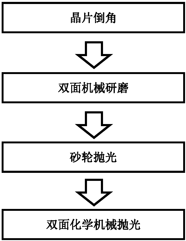
[0026] A kind of efficient processing method of silicon carbide wafer, its specific steps are as follows:

[0027] (1) Wafer chamfering;

[0028] (2) The chamfered wafer is ground on both sides, using a water-based diamond polishing fluid, the diamond particle size is 5 μm, the grinding pressure is 115 g / cm2, the grinding disc is a cast iron disc, and the surface of the cast iron disc is grooved. The interval is 10mm, the groove width is 1mm, the groove depth is 10mm, and the grinding time is 3.5h;

[0029] (3) Use automatic grinding wheel polishing equipment to grind and polish both sides of the wafer. First use a 5μm diamond grinding wheel with a rotation speed of 1500rpm, a grinding speed of 3μm / min, and a polishing time of 3 minutes; then use a 2μm diamond grinding wheel with a rotation speed of 2500rpm. The grinding speed is 1.5 μm / min, and the polishing time is 6 minutes; then a 1 μm diamond grinding wheel is used, the rotation speed is 3000 rpm, the grinding speed is 0...

Embodiment 2

[0035] A kind of efficient processing method of silicon carbide wafer, its specific steps are as follows:

[0036] (1) Wafer chamfering;

[0037] (2) The chamfered wafer is double-sidedly ground, using a water-based diamond polishing fluid, the diamond particle size is 3 μm, the grinding pressure is 160 g / cm2, the grinding disc is a cast iron disc, and the surface of the cast iron disc is grooved. The interval is 10mm, the groove width is 1mm, the groove depth is 10mm, and the grinding time is 3h;

[0038] (3) Use automatic grinding wheel polishing equipment to polish both sides of the wafer. First use a 10 μm diamond grinding wheel at a speed of 1000 rpm, a grinding speed of 5 μm / min, and a polishing time of 2 minutes; then use a 3 μm diamond grinding wheel at a speed of 2000 rpm. The grinding speed is 2 μm / min, and the polishing time is 8 minutes; then a 1 μm diamond grinding wheel is used, the rotation speed is 3000 rpm, the grinding speed is 0.3 μm / min, and the polishing ...

Embodiment 3

[0044] A kind of efficient processing method of silicon carbide wafer, its specific steps are as follows:

[0045] (1) Wafer chamfering;

[0046](2) The chamfered wafer is double-sidedly ground, using a water-based diamond polishing fluid, the diamond particle size is 5 μm, the grinding pressure is 160 g / cm2, the grinding disc is a cast iron disc, and the surface of the cast iron disc is grooved. The interval is 20mm, the groove width is 1mm, the groove depth is 10mm, and the grinding time is 3h;

[0047] (3) Use automatic grinding wheel polishing equipment to grind and polish both sides of the wafer. First use a 10μm diamond grinding wheel with a rotation speed of 800rpm, a grinding speed of 5μm / min, and a polishing time of 2 minutes; then use a 5μm diamond grinding wheel with a rotation speed of 1600rpm. The grinding speed is 2 μm / min, and the polishing time is 8 minutes; then a 2 μm diamond grinding wheel is used, the rotation speed is 3000 rpm, the grinding speed is 0.8 μ...


PUM

PropertyMeasurementUnit
particle diameteraaaaaaaaaa
particle sizeaaaaaaaaaa

Abstract

The invention belongs to the technical field of semiconductor material machining and particularly relates to an efficient silicon carbide wafer machining method. The machining method includes wafer chamfering, double-face mechanical lapping, grinding wheel polishing and double-face chemical mechanical polishing. By means of the efficient silicon carbide wafer machining method, diamond grinding wheel polishing is linked with double-face mechanical lapping and double-face chemical mechanical polishing, a waxed wafer attaching procedure in a traditional single-face machining method is abandoned,the machining technology process is greatly optimized, meanwhile, the automation degree and precision of wafer machining are improved, and silicon carbide wafers low in warping degree and high in surface quality are obtained. By means of the efficient silicon carbide wafer machining method, the wafer machining process is greatly simplified, the machining efficiency is improved, and commercializedlarge-scale production is facilitated.

Description

technical field [0001] The invention belongs to the technical field of semiconductor material processing, and relates to an efficient silicon carbide wafer processing method, which improves the processing quality and processing efficiency of the silicon carbide wafer, is beneficial to saving production and processing costs, and is suitable for industrialization promotion. Background technique [0002] With the rapid development of information technology today, the innovation of semiconductor technology plays an increasingly important role. Wide bandgap semiconductors represented by silicon carbide and gallium nitride are the third generation of wide bandgap semiconductors after silicon and gallium arsenide. Compared with traditional semiconductor materials represented by silicon and gallium arsenide, silicon carbide has great advantages in terms of operating temperature, breakdown voltage and radiation resistance. Silicon carbide has become the most mature wide-bandgap semi...

Claims


Application Information

Patent Timeline
Patent Type & Authority Applications(China)
IPC IPC(8): B24B1/00B24B7/22B24B37/005B24B37/04B24B37/08B24B37/16B24B27/00
CPCB24B1/00B24B7/228B24B27/0076B24B37/0056B24B37/044B24B37/08B24B37/16
Inventor 蔡振立刘春俊彭同华
Owner BEIJING TIANKE HEDA SEMICON CO LTD
Why Eureka
Try Eureka