Method for inducing periodic surface structure of transparent dielectric material with single-pulse nanosecond laser

A technology of periodic structures and dielectric materials, applied in nanostructure manufacturing, specific nanostructure formation, nanotechnology, etc., can solve problems such as cracks and high surface roughness, achieve the effect of changing optical characteristics and realizing information sensing

Inactive Publication Date: 2019-01-04
NANJING UNIV OF SCI & TECH +1
View PDF10 Cites 2 Cited by
  • Summary
  • Abstract
  • Description
  • Claims
  • Application Information

AI Technical Summary

Problems solved by technology

[0004] The purpose of the present invention is to propose a method for inducing a periodic structure on the surface of a transparent dielectric material by a single-pulse nanosecond laser to solve the problem of cracks and high surface roughness caused by the periodic structure on the surface of a transparent dielectric material prepared in the prior art Pit, or annular ablation topography

Method used


Image

  • Method for inducing periodic surface structure of transparent dielectric material with single-pulse nanosecond laser
  • Method for inducing periodic surface structure of transparent dielectric material with single-pulse nanosecond laser
  • Method for inducing periodic surface structure of transparent dielectric material with single-pulse nanosecond laser

Examples


Embodiment 1

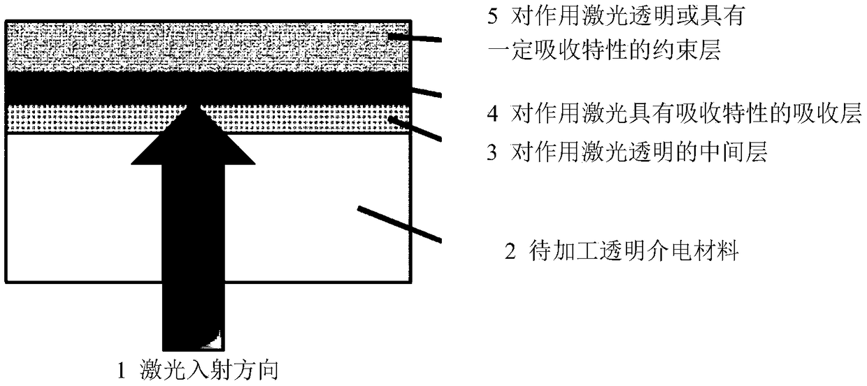
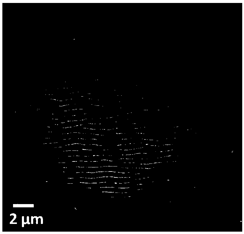
[0036] SiO 2 The etching process of LIPSS on the surface of the substrate is taken as an example to describe the technical solution of the present invention in detail.

[0037] (1) Using diameter 25cm, thickness 300μm, double-sided polished SiO 2 substrate.

[0038] (2) Spin-coating method on SiO 2 One side of the substrate was coated with a novolac resin (intermediate layer) in a thickness of 500 nm, followed by exposure to the novolak resin film and heating maintained at 150° C. for 1 minute to harden the novolak resin film. Finally, the novolac resin was etched to a thickness of 200 nm by Ar ion beam.

[0039] (3) A Cr film (absorbing layer) with a thickness of 100 nm was deposited on the surface of the novolac resin film by magnetron sputtering.

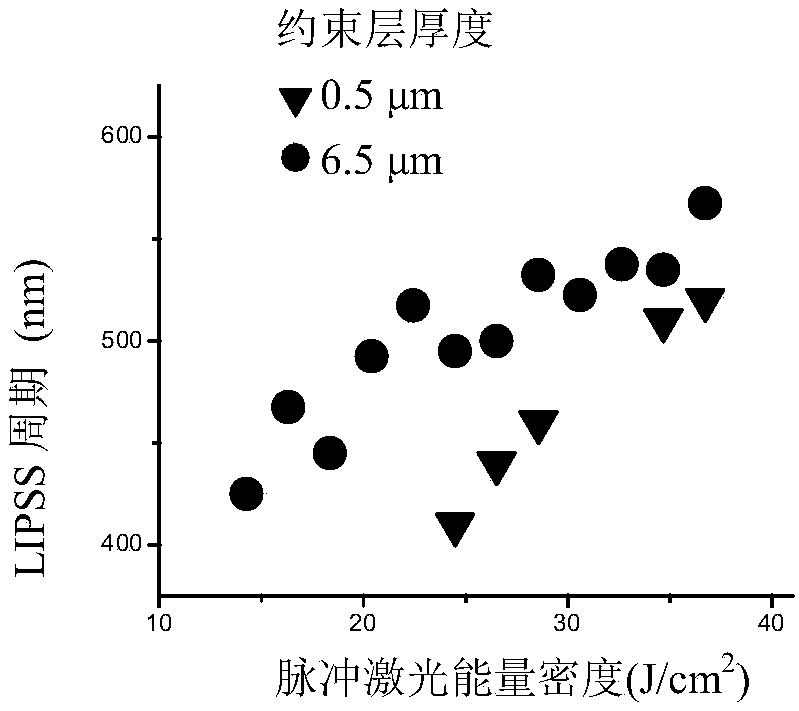
[0040] (4) Coating a 6.5 μm thick novolak resin film (constraint layer) on the surface of the Cr film by spin coating, then exposing the novolak resin film, and heating and maintaining it at 100° C. for 1 minute, so that the ...


PUM

PropertyMeasurementUnit
thicknessaaaaaaaaaa
thicknessaaaaaaaaaa
thicknessaaaaaaaaaa

Abstract

The present invention discloses a method for inducing a periodic surface structure of a transparent dielectric material with single-pulse nanosecond laser. The method comprises: covering a surface ofthe transparent dielectric material with an absorbing medium stack, wherein the absorbing medium stack comprises an intermediate layer disposed in contact with the transparent dielectric material andmade of a polymer which is transparent to the working laser or an oxide which is transparent to the working laser, and an absorbing layer covering a surface of the intermediate layer and made of C ora metal; allowing laser to penetrate the transparent dielectric material and the intermediate layer from one side, opposite to the side covered with the absorbing layer, of the transparent dielectricmaterial, and to be absorbed by the absorbing layer, so that the absorbing medium stack is removed and a laser-induced periodic surface structure (LIPSS) is formed on the surface of one side of the transparent dielectric material that is covered with the medium stack. According to the method for inducing a periodic surface structure of a transparent dielectric material with single-pulse nanosecondlaser, by making the LIPSS, the wetting property and the surface cell adhesion and growth characteristics of the material can be changed, and the catalytic reaction efficiency on the surface of the material can be regulated.

Description

technical field [0001] The invention relates to a technology for preparing a periodic structure on the surface of a transparent dielectric material, in particular to a method for inducing a periodic structure on the surface of a transparent dielectric material by a single-pulse nanosecond laser. Background technique [0002] Micro-nano-scale periodic structures (PSS) on the surface of dielectric materials have broad application prospects in the fields of optics, biology, electronics, medical treatment, and materials science. Methods for generating PSS can be divided into two categories. One is the direct shaping technology based on mask lithography, electron beam exposure, laser coherent lithography, and laser dry / wet etching. As we all know, this type of technology involves complex steps and processes, requires a vacuum processing environment, and sometimes requires the use of toxic and harmful chemical reagents or auxiliary gases. The other is to form PSS by virtue of th...

Claims


Application Information

Patent Timeline
Patent Type & Authority Applications(China)
IPC IPC(8): B82B3/00
CPCB82B3/0033
Inventor 马丁·伊尔哈特韩冰克劳斯·齐默朱日宏倪晓武
Owner NANJING UNIV OF SCI & TECH
Why Eureka
Try Eureka