Method of multi-pulse picosecond laser-induced semiconductor material periodic surface structure

A periodic structure and picosecond laser technology, applied in the process of producing decorative surface effects, microstructure technology, microstructure devices, etc., can solve the problems of harsh environmental conditions, expensive equipment, and complicated steps of periodic structures , to achieve the effect of easy operation and maintenance and cost reduction

Inactive Publication Date: 2020-06-09
NANJING UNIV OF SCI & TECH
View PDF6 Cites 3 Cited by
  • Summary
  • Abstract
  • Description
  • Claims
  • Application Information

AI Technical Summary

Problems solved by technology

[0003] The purpose of the present invention is to propose a method for inducing a periodic structure on the surface of semiconductor materials by multi-pulse picosecond lasers, which solves the problems of complex steps in preparing the surface periodic structures of semiconductor materials, harsh environmental conditions and expensive equipment in the prior art

Method used


Image

  • Method of multi-pulse picosecond laser-induced semiconductor material periodic surface structure
  • Method of multi-pulse picosecond laser-induced semiconductor material periodic surface structure
  • Method of multi-pulse picosecond laser-induced semiconductor material periodic surface structure

Examples


Embodiment 1

[0026] The technical scheme of the present invention is described in detail by taking the etching process of LIPSS on the surface of a Si substrate as an example.

[0027] (1) A Si substrate with a diameter of 2.5 cm and a thickness of 500 μm is used, which is polished on one side.

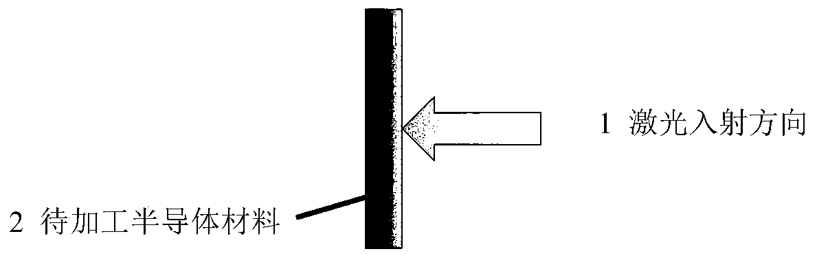
[0028] (2) A linearly polarized laser with a wavelength of 532 nm and a pulse width of 8 ps is selected as the active light source, and the laser is incident from the polished side (front side) of the Si substrate.

[0029] (3) Use a 150mm focal length lens to focus the laser beam so that the laser focus is located 10.5mm behind the polished surface.

[0030] (4) The laser energy density on the surface of the material is 0.17J / cm 2 .

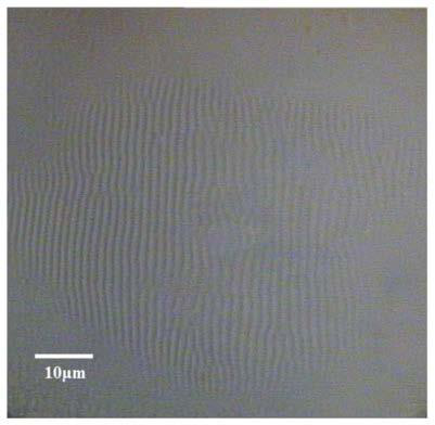
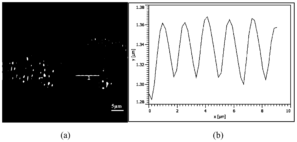
[0031] (5) Through 50 pulses of laser action, the intermediate layer, absorption layer and constrained layer medium in the laser irradiated area are removed at the same time, and the polished side surface on the Si substrate will produce LIPSS with a period betwee...


PUM

PropertyMeasurementUnit
thicknessaaaaaaaaaa
thicknessaaaaaaaaaa
wavelengthaaaaaaaaaa

Abstract

The invention provides a method of a multi-pulse picosecond laser-induced semiconductor material periodic surface structure. The method relates to a single-sided polished semiconductor material. According to the method, laser is vertically incident from the polishing surface of a semiconductor material and is absorbed on the surface of the semiconductor material, and a LIPSS is formed on the surface of one side of the polishing surface of the semiconductor material. The LIPSS prepared according to the method can alter the wetting characteristics and biocompatibility of the material, adjust theefficiency of material surface catalytic reaction, and change the optical characteristics of the surface of the material.

Description

technical field [0001] The invention relates to a technology for preparing a periodic structure on the surface of a semiconductor material, in particular to a method for inducing a periodic structure on the surface of a semiconductor material by a multi-pulse picosecond laser. Background technique [0002] The micro-nano-scale periodic structure (PSS) on the surface of semiconductor materials can change the optical, mechanical or chemical properties of materials, so it can be used in optics, electronics, tribology, medicine and other fields. To prepare the micro-nano-scale structure of the material surface, that is, to form a basic structural unit with a specific shape on the surface of the raw material by a certain method, and the size of this basic structural unit is controlled at the micron or nanometer level. Both the growth-based bottom-up method and the removal-based top-down method can realize the preparation of such basic building blocks on the material surface. For...

Claims


Application Information

Patent Timeline
Patent Type & Authority Applications(China)
IPC IPC(8): B23K26/362B23K26/0622B81C1/00
CPCB23K26/362B81C1/00444B81C1/00523B23K26/0624
Inventor 高语璠韩冰马丁·伊尔哈特于彩芸朱日宏
Owner NANJING UNIV OF SCI & TECH
Why Eureka
Try Eureka