A graphene-based plasmonic switch

A plasmon, graphene technology, applied in nanotechnology for materials and surface science, electrical components, sustainable manufacturing/processing, etc., can solve problems such as unexplored real spatial characteristics of limiting plasmon modes , to achieve the effect of long recovery time, enhanced interaction and fast response

Active Publication Date: 2020-11-27
同天(福建)石墨烯科技有限公司
View PDF9 Cites 0 Cited by
  • Summary
  • Abstract
  • Description
  • Claims
  • Application Information

AI Technical Summary

Problems solved by technology

Despite the well-characterized overall, area-averaged response of graphene nanostructures, the actual spatial properties of confined plasmonic modes in these nanostructures remain unexplored

Method used


Image

  • A graphene-based plasmonic switch
  • A graphene-based plasmonic switch
  • A graphene-based plasmonic switch

Examples


Embodiment 1

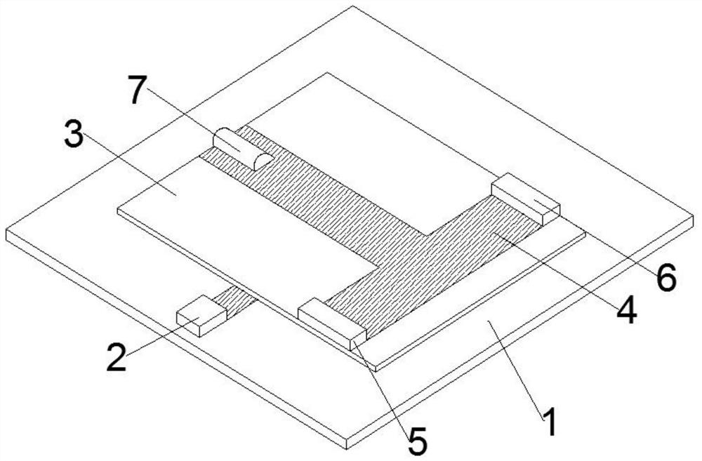
[0037]A graphene-based plasmonic switch, the graphene-based plasmonic switch includes a substrate layer 1, a hexagonal boron nitride substrate 3, a graphene nanoribbon 4, gold nanorods 7, a source 5, a drain Pole 6 and graphene gate, the upper surface of substrate layer 1 is provided with hexagonal boron nitride substrate 3, the upper surface of hexagonal boron nitride substrate 3 is provided with graphene nanobelt 4, graphene nanobelt 4 is arranged in a T-shaped structure, and the left side of the graphene nanoribbon 4 is provided with a gold nanorod 7, the front side is provided with a source 5, the rear side is provided with a drain 6, and the front side of the substrate layer 1 is provided with a graphene gate. pole.

[0038] Preferably, the substrate layer 1 is coated with a layer of Al 2 o 3 thin-film silicon substrate, and the thickness of the silicon substrate is 200 μm.

[0039] Preferably, the silicon substrate is SiO 2 base.

[0040] Preferably, the source elec...

Embodiment 2

[0051] A graphene-based plasmonic switch, the graphene-based plasmonic switch includes a substrate layer 1, a hexagonal boron nitride substrate 3, a graphene nanoribbon 4, gold nanorods 7, a source 5, a drain Pole 6 and graphene gate, the upper surface of substrate layer 1 is provided with hexagonal boron nitride substrate 3, the upper surface of hexagonal boron nitride substrate 3 is provided with graphene nanobelt 4, graphene nanobelt 4 is arranged in a T-shaped structure, and the left side of the graphene nanoribbon 4 is provided with a gold nanorod 7, the front side is provided with a source 5, the rear side is provided with a drain 6, and the front side of the substrate layer 1 is provided with a graphene gate. pole.

[0052] Preferably, the substrate layer 1 is coated with a layer of Al 2 o 3 thin-film silicon substrate, and the thickness of the silicon substrate is 300 μm.

[0053] Preferably, the silicon substrate is SiO 2 base.

[0054] Preferably, the source ele...

Embodiment 3

[0065] A graphene-based plasmonic switch, the graphene-based plasmonic switch includes a substrate layer 1, a hexagonal boron nitride substrate 3, a graphene nanoribbon 4, gold nanorods 7, a source 5, a drain Pole 6 and graphene gate, the upper surface of substrate layer 1 is provided with hexagonal boron nitride substrate 3, the upper surface of hexagonal boron nitride substrate 3 is provided with graphene nanobelt 4, graphene nanobelt 4 is arranged in a T-shaped structure, and the left side of the graphene nanoribbon 4 is provided with a gold nanorod 7, the front side is provided with a source 5, the rear side is provided with a drain 6, and the front side of the substrate layer 1 is provided with a graphene gate. pole.

[0066] Preferably, the substrate layer 1 is coated with a layer of Al 2 o 3 thin film silicon substrate, and the thickness of the silicon substrate is 400nm.

[0067] Preferably, the silicon substrate is SiO 2 base.

[0068] Preferably, the source elec...


PUM

PropertyMeasurementUnit
thicknessaaaaaaaaaa
diameteraaaaaaaaaa
thicknessaaaaaaaaaa

Abstract

The invention relates to the technical field of electronic devices and switches, in particular to a plasma exciton switch based on graphene. A graphene-based plasmon switch includes a substrate layer,A hexagonal boron nitride substrate, graphene nanobelt, gold nanorods, source, drain and graphene gate, the upper surface of the substrate layer is provided with a hexagonal boron nitride substrate,the upper surface of the hexagonal boron nitride substrate is provided with a graphene nanobelt, the graphene nanobelt is arranged in a T-shaped structure, and the left side of the graphene nanobelt is provided with a gold nanorod, the front side is provided with a source electrode, the rear side is provided with a drain electrode, and the front side of the substrate layer is provided with a graphene grid; The graphene plasma exciton switch prepared by the invention utilizes p-polarized infrared absorption spectrum technology and the characteristic advantages of the graphene plasma exciton andthe like, and has the advantages of strong light absorption capacity, fast response speed and the like.

Description

technical field [0001] The invention relates to the technical field of electronic devices and switches, in particular to a graphene-based plasmon switch. Background technique [0002] Graphene is a carbon atom with sp 2 The hybrid orbitals form a hexagonal planar film with a honeycomb lattice. Due to the linear energy band structure dispersion near the Dirac point and the extremely high carrier mobility of both electrons and holes, graphene presents a peculiar electronic Properties, such as the quantum spin Hall effect, graphene has attracted considerable attention as a next-generation semiconductor material for the above-mentioned reasons. Compared with traditional silicon-based transistor preparation materials, graphene has excellent mechanical, thermal, optical and electrical properties. These excellent properties of graphene make it have great application potential in the fields of electronic devices and optoelectronic devices. [0003] Surface plasmon polaritons, coll...

Claims


Application Information

Patent Timeline
Patent Type & Authority Patents(China)
IPC IPC(8): H01L31/028H01L31/113H01L31/18B82Y30/00B82Y40/00
CPCB82Y30/00B82Y40/00H01L31/028H01L31/1136H01L31/1804Y02P70/50
Inventor 朱授恩
Owner 同天(福建)石墨烯科技有限公司
Why Eureka
Try Eureka