A method for manufacturing a pyroelectric infrared detector sensing unit
A pyroelectric infrared, sensitive unit technology, applied in electrical components, circuits, semiconductor devices, etc., can solve problems such as difficulty in preparing high-performance pyroelectric infrared detectors, weak absorption layer adhesion, and narrow absorption band. , to achieve the effect of excellent heat transfer performance, small specific heat capacity and wide absorption band
- Summary
- Abstract
- Description
- Claims
- Application Information
AI Technical Summary
Problems solved by technology
Method used
Image

Examples
example 1
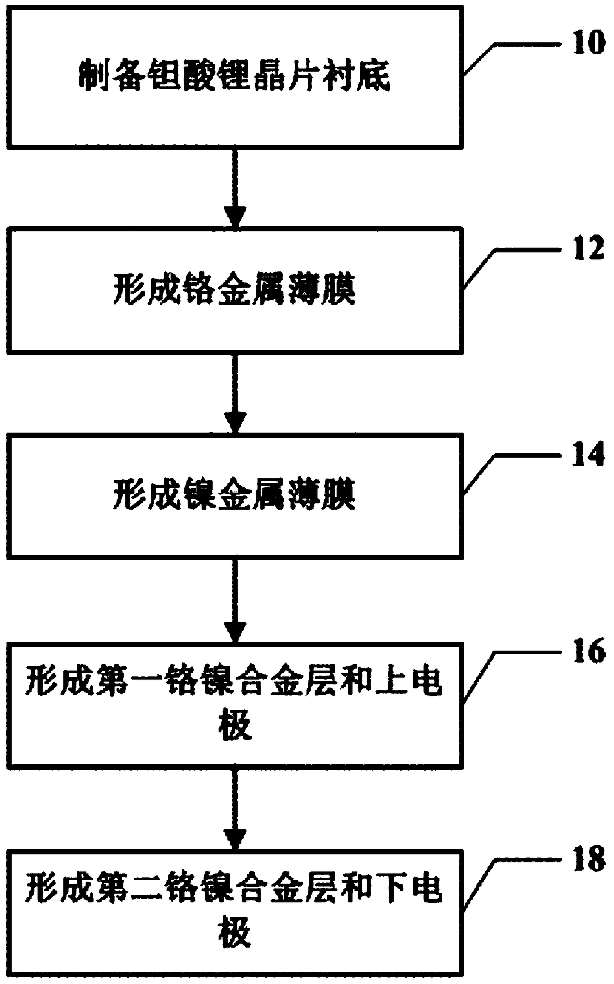
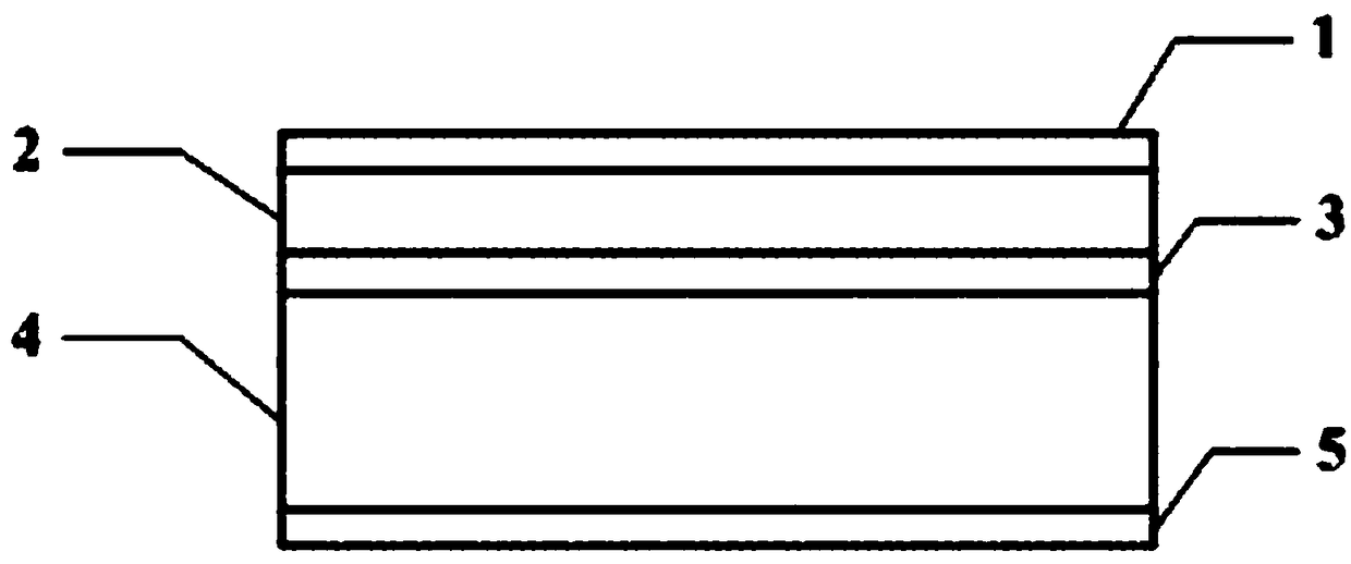
[0043] (1) Lithium tantalate (LiTaO3) crystal surface treatment
[0044] 1) Clean the LiTaO3 wafer. Carry out mechanical thinning polishing and chemical etching to LiTaO3 wafer A surface (first surface) and B surface (second surface). Wet etching of LiTaO3 wafers to remove defects and damage from thinning and polishing.
[0045] (2) Deposit the infrared absorbing layer and etch to form the electrode structure
[0046] 2) Clean the LiTaO3 wafer, and pattern it by photolithography on the A side (that is, form the pattern described above).
[0047] 3) Depositing a chromium metal film and a nickel metal film on the A side of the LiTaO3 wafer by magnetron sputtering. Float cleaning. Among them, the thickness of the chromium metal film is 15nm, and the thickness of the nickel metal film is 60nm.
[0048] 4) Photolithographic patterning on the A side of the LiTaO3 wafer.
[0049] 5) Deposit a chromium-nickel alloy absorbing layer on the A side of the LiTaO3 wafer by magnetron s...
example 2
[0056] (1) LiTaO3 surface treatment
[0057] 1) Clean the LiTaO3 wafer. Carry out mechanical thinning polishing and chemical etching to LiTaO3 wafer A surface (first surface) and B surface (second surface). Wet etching of LiTaO3 wafers to remove defects and damage from thinning and polishing.
[0058] (2) Deposit the infrared absorbing layer and etch to form the electrode structure
[0059] 2) Clean the LiTaO3 wafer, and pattern it by photolithography on the A side.
[0060] 3) On the A side of the LiTaO3 wafer, a magnetron sputtering process is used to deposit a chromium metal film and a nickel metal film, and the floating glue is cleaned. Among them, the thickness of the chromium metal film is 20nm, and the thickness of the nickel metal film is 65nm.
[0061] 4) Photolithographic patterning on the A side of the LiTaO3 wafer.
[0062] 5) Deposit a chromium-nickel alloy absorbing layer on the A side of the LiTaO3 wafer by thermal evaporation. The sheet resistance of the c...
PUM
| Property | Measurement | Unit |
|---|---|---|
| Thickness | aaaaa | aaaaa |
| Thickness | aaaaa | aaaaa |
| Thickness | aaaaa | aaaaa |
Abstract
Description
Claims
Application Information
 - R&D
- Intellectual Property
- Life Sciences
- Materials
- Tech Scout
- Unparalleled Data Quality
- Higher Quality Content
- 60% Fewer Hallucinations
Browse by: Latest US Patents, China's latest patents, Technical Efficacy Thesaurus, Application Domain, Technology Topic, Popular Technical Reports.
© 2025 PatSnap. All rights reserved.Legal|Privacy policy|Modern Slavery Act Transparency Statement|Sitemap|About US| Contact US: help@patsnap.com