A wide-spectrum inorganic perovskite solar cell structure and its preparation method
A technology of solar cells and inorganic calcium, applied in the field of solar cells, can solve the problems of narrow spectral absorption range, low efficiency of inorganic perovskite solar cells, wide band gap, etc., to improve efficiency, increase absorption, improve spectral utilization and light Effect of Raw Carrier Extraction Efficiency
- Summary
- Abstract
- Description
- Claims
- Application Information
AI Technical Summary
Problems solved by technology
Method used
Image
Examples
Embodiment 1
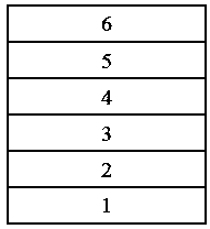
[0024] Such as figure 1 As shown, the structure of a wide-spectrum inorganic perovskite solar cell is conductive glass-1, photoanode layer-2, electron transport layer-3, perovskite light-absorbing layer-4, and photoactivation layer-5 from top to bottom. , Electrode layer-6.
[0025] (1) Conductive glass 1 composed of transparent glass and FTO was ultrasonically cleaned with acetone, isopropanol, and deionized water for 10 to 20 minutes, then dried with nitrogen flow, and then the conductive glass 1 was treated with ultraviolet and ozone for 20 minutes. ~30 minutes.
[0026] (2) Prepare the photoanode layer 2 on the conductive glass 1 . A layer of dense titanium dioxide was coated on conductive glass using the sol-gel method.
[0027] (3) The electron transport layer 3 is prepared on the photoanode layer 2 . A layer of mesoporous titania was prepared on dense titania using a hydrothermal method.
[0028] (4) Prepare the perovskite light absorbing layer 4 on the electron tr...
Embodiment 2
[0032] Such as figure 1 As shown, the structure of a wide-spectrum inorganic perovskite solar cell is conductive glass-1, photoanode layer-2, electron transport layer-3, perovskite light-absorbing layer-4, and photoactivation layer-5 from top to bottom. , electrode layer-6.
[0033] (1) Conductive glass 1 composed of transparent glass and FTO was ultrasonically cleaned with acetone, isopropanol, and deionized water for 10 to 20 minutes, then dried with nitrogen flow, and then the conductive glass 1 was treated with ultraviolet and ozone for 20 minutes. ~30 minutes.
[0034] (2) Prepare the photoanode layer 2 on the conductive glass 1 . A layer of dense titanium dioxide was coated on conductive glass using the sol-gel method.
[0035] (3) The electron transport layer 3 is prepared on the photoanode layer 2 . A layer of mesoporous titania was prepared on dense titania using a hydrothermal method.
[0036] (4) Prepare the perovskite light absorbing layer 4 on the electron tr...
example 3
[0040] Such as figure 1 As shown, the structure of a wide-spectrum inorganic perovskite solar cell is conductive glass-1, photoanode layer-2, electron transport layer-3, perovskite light-absorbing layer-4, and photoactivation layer-5 from top to bottom. , electrode layer-6.
[0041] (1) Conductive glass 1 composed of transparent glass and FTO was ultrasonically cleaned with acetone, isopropanol, and deionized water for 10 to 20 minutes, then dried with nitrogen flow, and then the conductive glass 1 was treated with ultraviolet and ozone for 20 minutes. ~30 minutes.
[0042] (2) Prepare the photoanode layer 2 on the conductive glass 1 . A layer of dense titanium dioxide was coated on conductive glass using the sol-gel method.
[0043] (3) The electron transport layer 3 is prepared on the photoanode layer 2 . A layer of mesoporous titania was prepared on dense titania using a hydrothermal method.
[0044] (4) Prepare the perovskite light absorbing layer 4 on the electron tr...
PUM
| Property | Measurement | Unit |
|---|---|---|
| thickness | aaaaa | aaaaa |
Abstract
Description
Claims
Application Information
