A wide-band photodetector of perovskite thin film based on topological insulator bismuth selenide electrode and a preparation method thereof

A photodetector, topological insulator technology, applied in semiconductor/solid-state device manufacturing, electric solid-state devices, semiconductor devices, etc., can solve the problems of complex graphene electrode fabrication and transfer process, hindering charge carrier transport, and poor flexibility of ITO electrodes. , to achieve the effect of long charge diffusion length, low defect density and good device performance

Active Publication Date: 2019-01-18
HEFEI UNIV OF TECH
View PDF4 Cites 8 Cited by
  • Summary
  • Abstract
  • Description
  • Claims
  • Application Information

AI Technical Summary

Problems solved by technology

The selection of electrode materials plays an important role in photodetectors. Traditional photodetector electrode materials, such as noble metals such as gold, silver, and platinum, are expensive, and there are considerable dangling bonds on their irregular surfaces, which may lead to Severe carrier scattering and impeded transport of charge carriers
At present, some oxide electrodes (such as ITO) or graphene electrodes are more and more applied to optoelectronic devices because of their own advantages, but due to the poor flexibility of ITO electrodes and low transmittance in the infrared region, the production of graphene electrodes The complexity of the transfer process also limits the application of both

Method used


Image

  • A wide-band photodetector of perovskite thin film based on topological insulator bismuth selenide electrode and a preparation method thereof
  • A wide-band photodetector of perovskite thin film based on topological insulator bismuth selenide electrode and a preparation method thereof
  • A wide-band photodetector of perovskite thin film based on topological insulator bismuth selenide electrode and a preparation method thereof

Examples


Embodiment 1

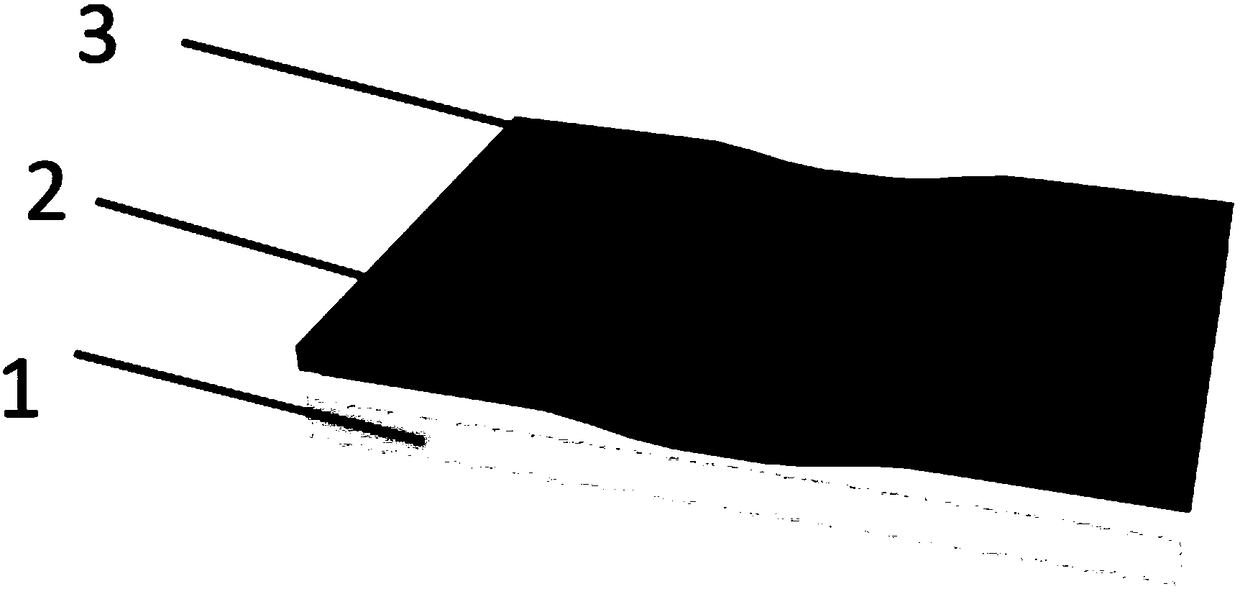
[0031] See figure 1 , The photodetector of the present invention is provided with Bi on the sapphire substrate 1 2 Se 3 Thin film electrode 2, in Bi 2 Se 3 A layer of FA is provided on the film electrode 2 0.85 Cs 0.15 PbI 3 Perovskite film 3.

[0032] Specifically: Bi in this embodiment 2 Se 3 The thin-film electrode first grows a layer of Bi on a sapphire substrate by molecular beam epitaxy. 2 Se 3 The thin film is then etched by ultraviolet exposure lithography and oxygen plasma cleaning machine to remove Bi 2 Se 3 The thin film is etched into the required electrode pattern to obtain. Bi 2 Se 3 The thickness of the thin film electrode is between 80 and 90 nm.

[0033] Specifically: FA in this embodiment 0.85 Cs 0.15 PbI 3 The perovskite film is made of lead iodide PbI 2 , Cesium iodide CsI, formamidine hydroiodic acid FAI dissolved in dimethyl sulfoxide DMSO and N, N-dimethylformamide DMF to form a precursor solution, through the homogenizer in the growth of Bi 2 Se 3 The thin-fi...


PUM

PropertyMeasurementUnit
thicknessaaaaaaaaaa
thicknessaaaaaaaaaa

Abstract

The invention discloses a wide-band photodetector of A perovskite thin film based on A topological insulator bismuth selenide electrode and a preparation method thereof. A Bi2Se3 thin film electrode is arranged on a sapphire substrate, and a layer of FA0. 85Cs0. 15PbI3 perovskite thin film is arranged on that Bi2Se3 thin film electrode. The invention utilizes the characteristic of large specific surface area of perovskite thin film and the special conductive surface state of topological insulator, a The response of the photodetector is sensitive in the range of UV- visible-near infrared light.The detector of the invention has simple preparation process and good device performance, and opens up new prospects for the application of topological insulator material in photoelectric detectors.

Description

Technical field [0001] The invention belongs to the field of semiconductor photodetectors, and specifically relates to a topological insulator Bi 2 Se 3 A wide-band high-performance photodetector with perovskite film electrodes. Background technique [0002] Photodetectors are widely used in optical communications, imaging, and biosensing because they can convert optical signals into electrical signal output. The selection of electrode materials plays an important role in photodetectors. Traditional photodetector electrode materials such as precious metals gold, silver, platinum, etc. are expensive, and there are quite large dangling bonds on their irregular surfaces, which may lead to Severe carrier scattering and hinder the transport of charge carriers. At present, some oxide electrodes (such as ITO) or graphene electrodes are increasingly used in optoelectronic devices due to their own advantages. However, due to the poor flexibility of ITO electrodes and low transmittance in...

Claims


Application Information

Patent Timeline
Patent Type & Authority Applications(China)
IPC IPC(8): H01L51/42H01L51/44H01L51/46H01L51/48
CPCH10K71/12H10K85/30H10K30/00H10K30/81Y02E10/549
Inventor 梁凤霞梁林赵兴远罗林保张致翔
Owner HEFEI UNIV OF TECH
Why Eureka
Try Eureka