Lead-free all-inorganic perovskite cesium bismuth iodide thin film/n-type silicon heterojunction photodetector and preparation method thereof

A technology of photodetectors and silicon heterojunctions, applied in the field of photodetectors, can solve problems such as poor stability, toxicity, and hindering the application of materials, and achieve the effects of good stability, fast response speed, and reduced production costs

Pending Publication Date: 2019-01-22
HEFEI UNIV OF TECH
View PDF10 Cites 5 Cited by
  • Summary
  • Abstract
  • Description
  • Claims
  • Application Information

AI Technical Summary

Problems solved by technology

However, the common lead halide perovskite materials have poor stability in the a

Method used


Image

  • Lead-free all-inorganic perovskite cesium bismuth iodide thin film/n-type silicon heterojunction photodetector and preparation method thereof
  • Lead-free all-inorganic perovskite cesium bismuth iodide thin film/n-type silicon heterojunction photodetector and preparation method thereof
  • Lead-free all-inorganic perovskite cesium bismuth iodide thin film/n-type silicon heterojunction photodetector and preparation method thereof

Examples


Embodiment 1

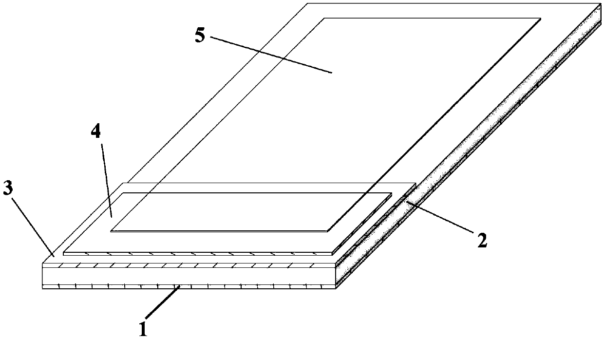
[0032] Such as figure 1 Shown, in this embodiment perovskite CsBi 3 I 10 The structure of the thin film / n-type silicon heterojunction photodetector is as follows: the n-type silicon substrate 2 is used as the base region of the photodetector, and the n-type silicon substrate electrode 1 is arranged on the lower surface of the n-type silicon substrate 2; Cover the upper surface of the n-type silicon substrate 2 with an insulating layer 3, the area of ​​the insulating layer 3 is 1 / 5 to 2 / 3 of the area of ​​the n-type silicon substrate 2, and the boundary of the insulating layer 3 does not exceed the n-type silicon substrate 2 The boundary; on the insulating layer 3 covered perovskite CsBi 3 I 10 Thin film contact electrode 4, perovskite CsBi 3 I 10 The boundary of the film contact electrode 4 does not exceed the boundary of the insulating layer 3; in the perovskite CsBi 3 I 10 Perovskite CsBi is laid on the film contact electrode 4 3 I 10 Thin film 5, perovskite CsBi 3...

Embodiment 2

[0044] Such as figure 1 Shown, in this embodiment perovskite CsBi 3 I 10 The structure of the thin film / n-type silicon heterojunction photodetector is as follows: the n-type silicon substrate 2 is used as the base region of the photodetector, and the n-type silicon substrate electrode 1 is arranged on the lower surface of the n-type silicon substrate 2; Cover the upper surface of the n-type silicon substrate 2 with an insulating layer 3, the area of ​​the insulating layer 3 is 1 / 5 to 2 / 3 of the area of ​​the n-type silicon substrate 2, and the boundary of the insulating layer 3 does not exceed the n-type silicon substrate 2 The boundary; on the insulating layer 3 covered perovskite CsBi 3 I 10 Thin film contact electrode 4, perovskite CsBi 3 I 10 The boundary of the film contact electrode 4 does not exceed the boundary of the insulating layer 3; in the perovskite CsBi 3 I 10 Perovskite CsBi is laid on the film contact electrode 4 3 I 10 Thin film 5, perovskite CsBi 3...


PUM

PropertyMeasurementUnit
Thicknessaaaaaaaaaa
Thicknessaaaaaaaaaa
Thicknessaaaaaaaaaa

Abstract

The invention discloses a lead-free all-inorganic perovskite cesium bismuth iodide thin film/n-type silicon heterojunction photodetector and a preparation method thereof. The n-type silicon substrateis used as the base region of the photodetector, and the n-type silicon base electrode is disposed on the lower surface of the n-type silicon substrate; the upper surface of the n-type silicon substrate is covered with the insulating layer, and the insulating layer is covered with calcium Titanium ore CsBi3I10 film contact electrode, a perovskite CsBi3I10 film is deposited on the perovskite CsBi3I10 film contact electrode, and a part of the film forms an ohmic contact with the perovskite CsBi3I10 film contact electrode, and the remaining portion and the n-type silicon substrate surface are notcovered with the insulating layer to form a HeterojunctionThe photoelectric detector of the invention has the advantages of simple process, low cost, stable property, large current switching ratio and fast response speed.

Description

technical field [0001] The invention belongs to the technical field of photodetectors, in particular to a perovskite CsBi 3 I 10 Thin film / n-type silicon heterojunction photodetectors and methods of making the same. Background technique [0002] A photodetector is an optoelectronic device that converts light signals into electrical signals. Low-cost high-performance photodetectors have important application value in many scientific research and industrial technology fields including image sensing, optical communication, fire detection, biomedical imaging, environmental monitoring, space detection and safety detection, so they have been widely s concern. [0003] At present, in the widely used visible-near-infrared light band (wavelength <1100nm), photodetectors based on crystalline silicon occupy a major market share. Thanks to mature processing technology and good compatibility with silicon-based CMOS technology, people have successfully developed a variety of silico...

Claims


Application Information

Patent Timeline
IPC IPC(8): H01L51/42H01L51/46H01L51/48
CPCH10K71/12H10K85/30H10K30/10Y02E10/549
Inventor 罗林保童小伟张轶尧林亚楠黄瑞
Owner HEFEI UNIV OF TECH
Why Eureka
Try Eureka