A kind of preparation method of p+/p/n antimony selenide thin film battery
A thin film battery, antimony selenide technology, applied in circuits, electrical components, photovoltaic power generation and other directions, can solve the problems of low carrier concentration of antimony selenide, restricting development, and hindering efficiency, achieving low cost, promoting development, The effect of high degree of industrialization
- Summary
- Abstract
- Description
- Claims
- Application Information
AI Technical Summary
Problems solved by technology
Method used
Image

Examples
Embodiment 1
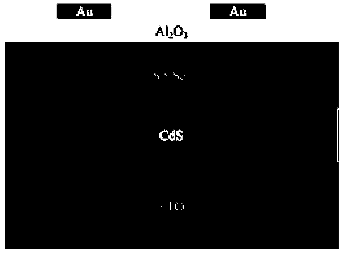
[0020] 1. The substrate is made of FTO glass, which is ultrasonically cleaned with alkaline solution, acetone, ethanol, and deionized water in sequence, and dried for later use.
[0021] 2. Preparation of N-type CdS thin film
[0022] CdSO 4 Solution 15mL, ammonia water 19mL, and thiourea solution 15mL were poured into a beaker filled with 250mL deionized water and mixed uniformly to obtain a blended solution. Clamp the cleaned FTO glass into the blended solution and stir solution, the reaction time is 20min, the reaction temperature is 70°C, and a CdS film with a thickness of about 40nm is obtained, dried by ultrasonic wave and placed in an oxygen plasma machine, and treated with oxygen plasma for 15min to obtain a processed N-type CdS film.
[0023] 3. P-type Sb 2 Se 3 Film preparation
[0024] (1) Put the above-mentioned treated N-type CdS film into the Sb 2 Se 3 In the powder rapid annealing furnace, the cavity pressure is evacuated to 0.34Pa by using a vacuum pump. ...
Embodiment 2
[0039] 1. The substrate is made of FTO glass, which is ultrasonically cleaned with alkaline solution, acetone, ethanol, and deionized water in sequence, and dried for later use.
[0040] 2. Preparation of N-type CdS thin film
[0041] CdSO 4 Solution 20mL, ammonia water 35mL, thiourea solution 25mL, pour into a beaker filled with 300mL deionized water and mix evenly to obtain a mixed solution, clamp the cleaned FTO glass into the mixed solution, and stir the solution, The reaction time was 30 minutes, and the reaction temperature was 65°C to obtain a CdS film with a thickness of about 50 nm, which was dried by ultrasonic and placed in an oxygen plasma machine, and treated with oxygen plasma for 30 minutes to obtain a processed N-type CdS film.
[0042] 3. P-type Sb 2 Se 3 Film preparation
[0043] (1) Put the above-mentioned treated N-type CdS film into the Sb 2 Se 3 In the powder rapid annealing furnace, the chamber pressure is evacuated to below 0.34Pa by using a vacuu...
PUM
| Property | Measurement | Unit |
|---|---|---|
| thickness | aaaaa | aaaaa |
| thickness | aaaaa | aaaaa |
| thickness | aaaaa | aaaaa |
Abstract
Description
Claims
Application Information