

Non-polar InAlN/GaN high electron mobility transistor and preparation method thereof
A high electron mobility, non-polar technology, applied in the field of microelectronics, can solve problems affecting device stability, reliability hazards, material and device damage, etc., to suppress the generation of high-density polarized charges and improve process repetition Performance and stability, guaranteed performance and reliability
- Summary
- Abstract
- Description
- Claims
- Application Information
AI Technical Summary
Problems solved by technology
Method used
Image

Examples
Embodiment 1
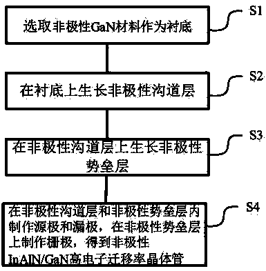
[0048] See figure 1 , figure 1 A flowchart of a method for fabricating a non-polar InAlN / GaN high electron mobility transistor provided in an embodiment of the present invention includes the following steps:
[0049] S1. Selecting a non-polar GaN material as the substrate 101;
[0050] S2, growing GaN on the substrate to form a non-polar channel layer;
[0051] S3, growing InAlN on the non-polar channel layer to form a non-polar barrier layer;
[0052] S4. Fabricate source and drain electrodes in the nonpolar channel layer and the nonpolar barrier layer, and fabricate a gate on the nonpolar barrier layer to obtain the nonpolar InAlN / GaN high electron mobility transistors.
[0053] Specifically, after step S1, it also includes:
[0054] S11. Perform nitriding treatment on the substrate at a temperature ranging from 828°C to 1012°C; preferably, the treatment temperature is 920°C;
[0055] S12. Processing the substrate, the processing process is: growing a GaN film on the ...
Embodiment 2
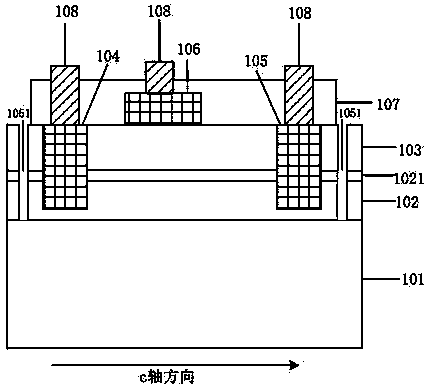
[0076] See figure 2 , figure 2 A schematic diagram of the structure of a non-polar InAlN / GaN high electron mobility transistor provided for the embodiment of the present invention. On the basis of the first embodiment above, the purchased semi-insulating non-polar a-plane homogeneous GaN material is used as the substrate 101. Preparation of non-polar InAlN / GaN high electron mobility transistors, wherein the semi-insulating non-polar a-plane homogeneous GaN material is grown by hydride vapor phase epitaxy (HVPE for short) .
[0077] In the embodiment of the present invention, a non-polar GaN homogeneous material based on a new type of hydride vapor phase epitaxy is selected as the substrate, which can not only effectively alleviate the difficulty of epitaxially growing non-polar materials on heterogeneous materials, but also improve the crystallization quality of epitaxial materials. , the transport properties of heterostructures and the working performance of HEMTs devices...
Embodiment 3
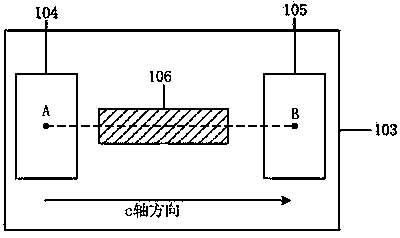
[0120] On the basis of Embodiment 1 and Embodiment 2, the angle between the gate direction and the c-axis direction of the non-polar InAlN / GaN high electron mobility transistor in this embodiment is 45°, please refer to Figure 4 and Figure 5 , Figure 4 A schematic structural diagram of another non-polar InAlN / GaN high electron mobility transistor provided by an embodiment of the present invention, Figure 5 A schematic diagram of the c-axis direction and the gate direction of another non-polar InAlN / GaN high electron mobility transistor provided by an embodiment of the present invention.
[0121] Specific steps are as follows:
[0122] For steps S1-S3, please refer to Embodiment 2;
[0123] S41. Depositing a metal material on the non-polar barrier layer 203 by using a metal evaporation method to form a source electrode 204 and a drain electrode 205;
[0124] First, photoetching the source electrode region and the drain electrode region on the non-polar barrier layer 203; ...
PUM
| Property | Measurement | Unit |
|---|---|---|
| Thickness | aaaaa | aaaaa |
Abstract
Description
Claims
Application Information