HTCC system-level package structure and package method of flip chip

A system-level packaging and packaging structure technology, which is applied in the manufacturing of electrical components, electrical solid-state devices, semiconductor/solid-state devices, etc., can solve the problems of inability to meet complex system circuit integration, damage to the atmosphere inside the sealed cavity, and affect chip reliability. , to achieve broad market application prospects, improve system integration, and protect reliability.

Active Publication Date: 2019-03-01
XIAN INSTITUE OF SPACE RADIO TECH
View PDF8 Cites 11 Cited by
  • Summary
  • Abstract
  • Description
  • Claims
  • Application Information

AI Technical Summary

Problems solved by technology

[0004] Since the flip chip under the HTCC process needs to be underfilled after installation, the filler will volatilize organic gas, destroy the atmosphere inside the sealed cavity, and affect the reliability of other chips. The heat dissipation path, so the existing method is to independently place the flip-chip on the front of the HTCC substrate, and no longer place other chips. Only the flip-chip occupies the main area of ​​the substrate, and the system integration level is low, which cannot meet Complex System Circuit Integration Requirements

Method used


Image

  • HTCC system-level package structure and package method of flip chip
  • HTCC system-level package structure and package method of flip chip
  • HTCC system-level package structure and package method of flip chip

Examples


preparation example Construction

[0027] A method for preparing a flip chip HTCC system-in-package structure. The steps of the method include:

[0028] (1) To prepare the HTCC substrate 1, the length and width of the HTCC substrate 1 shall be 35-60mm, the thickness shall be 2-4mm, and the flatness of the flip chip mounting area shall not be greater than 30μm;

[0029] (2) To prepare the upper cavity enclosure frame 2 and the lower cavity enclosure frame 4, the height of the upper cavity enclosure frame 2 is 1.5-3mm, the height of the lower cavity enclosure frame 4 is 1.5-2mm; the upper cavity enclosure frame 2 and the lower cavity enclosure frame 4 have a wall thickness of 1-2mm, and the upper cavity enclosure frame 2 and the lower cavity enclosure frame 4 are made of Kovar alloy;

[0030] (3) Prepare the upper cavity cover 3 and the lower cavity cover 5, the upper cavity cover 3 and the lower cavity cover 5 are made of Kovar alloy, the upper cavity cover 3 and the lower cavity cover The thickness of the plate 5 is ...

Embodiment

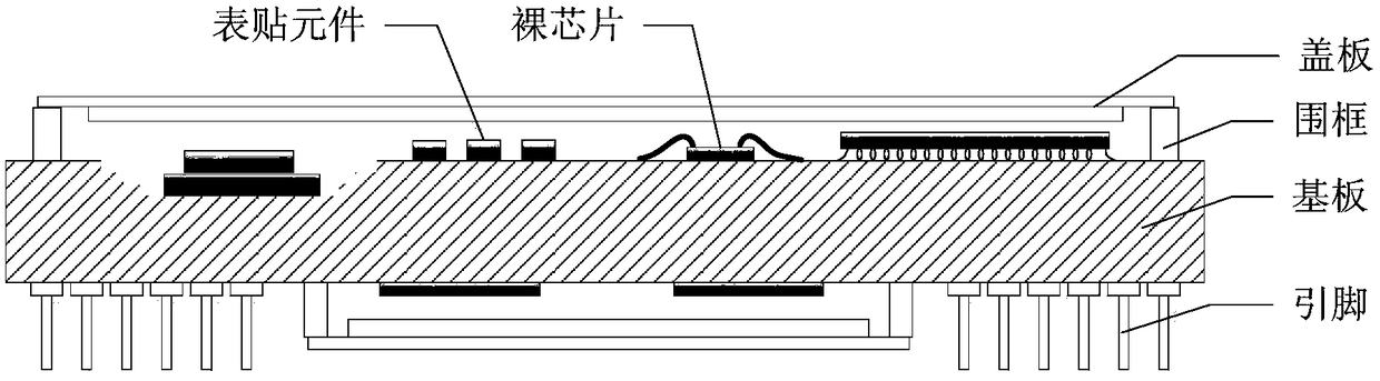
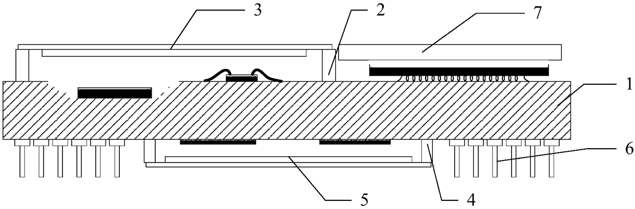
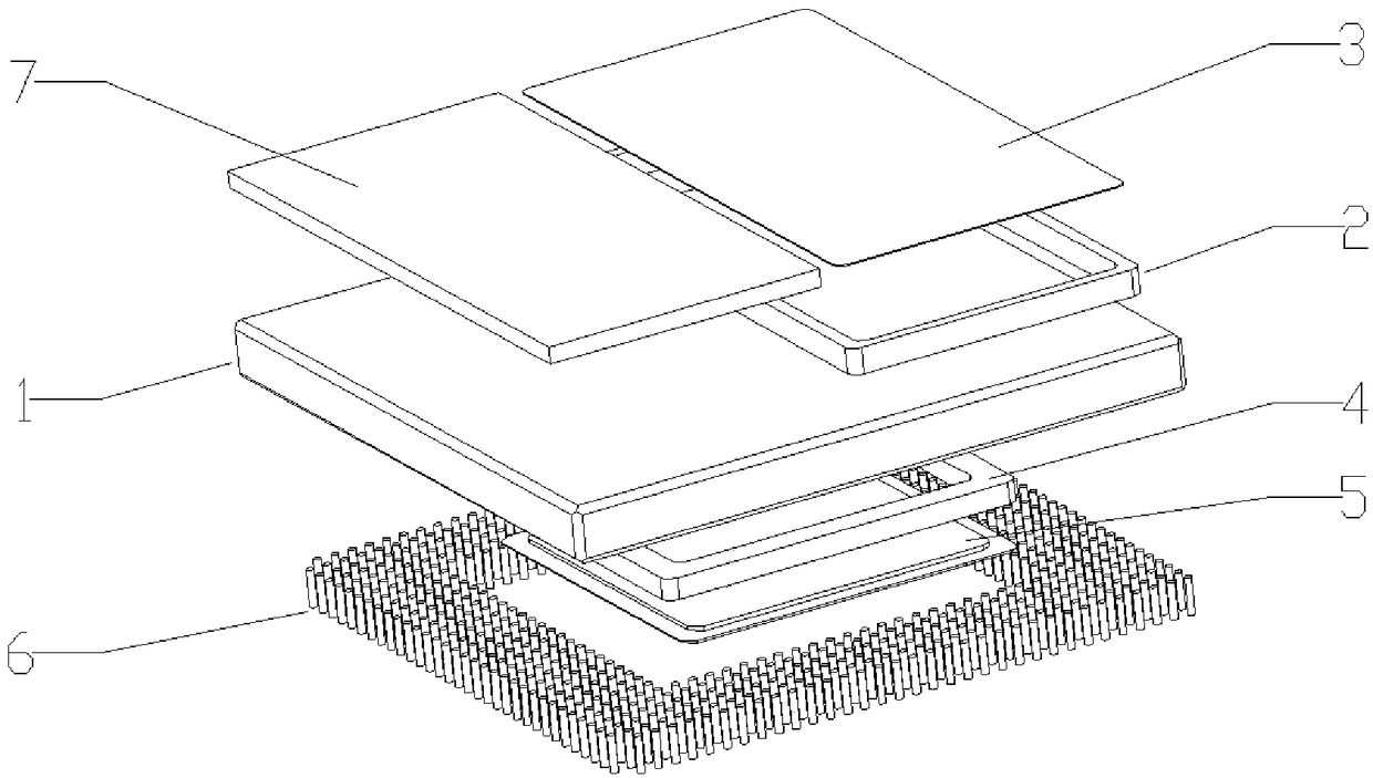
[0037] Such as figure 2 with image 3 As shown, a flip chip HTCC system-in-package structure includes an HTCC substrate 1, an upper cavity enclosure frame 2, an upper cavity cover plate 3, a lower cavity enclosure frame 4, and a lower cavity cover plate 5. CGA pin array 6 and heat sink 7;

[0038] The heat sink 7 and the upper cavity cover plate 3 are placed side by side on the upper surface of the HTCC substrate 1. Between the HTCC substrate 1 and the heat sink 7 is the mounting area for the flip-chip chip. Between the HTCC substrate 1 and the upper cavity cover plate 3 The upper cavity enclosure frame 2 is installed between the HTCC substrate 1, the upper cavity cover plate 3 and the upper cavity enclosure frame 2 to form a closed cavity; the CGA pin array 6 has a cavity in the center, and the lower cavity The cover plate 5 is installed in the central cavity of the CGA pin array 6. The CGA pin array 6 and the lower cavity cover plate 5 are located on the lower surface of the ...


PUM


Abstract

The invention relates to an HTCC system-level package structure and package method of a flip chip, in particular to an HTCC integrated system-level package structure applicable to a large-power consumption flip chip, and belongs to the technical field of system-level package. Large power consumption means that the power consumption of the flip chip is not smaller than 10W. Compared with an existing package structure, the digital-analog hybrid high-integration HTCC integrates system-level package structure applicable to the large-power consumption flip chip has the advantages that the problemsof compatibility of cooling, flip-chip bonding and a gold wire bonding process of the large-power consumption chip are solved, the system integration is also improved by a dual-sealing cavity design,the demand of satellite-borne digital ceramic system-level package is satisfied, and the HTCC system-level package structure has relatively high practicability and wide market application prospect.

Description

Technical field [0001] The present invention relates to a HTCC system-level packaging structure and packaging method for flip-chip welding chips, and in particular to a HTCC integrated system-level packaging structure suitable for high-power flip-chips. The high power consumption refers to The power consumption of the soldered chip is not less than 10W, which belongs to the field of system-in-package technology. Background technique [0002] In recent years, in the face of increasingly stringent requirements for weight, volume, and autonomous control of aerospace loads, System in Package (SiP) technology provides an effective way to achieve load integration, miniaturization, and light weight. Solutions. Because high temperature co-fired ceramics (HTCC) have the advantages of high structural strength, high thermal conductivity, good chemical stability and high wiring density, they are widely used in satellite-borne digital systems and packaging circuits. At present, the commonly...

Claims


Application Information

Patent Timeline
Patent Type & Authority Applications(China)
IPC IPC(8): H01L21/56H01L23/31H01L23/367H01L23/498H01L25/065
CPCH01L21/563H01L23/3121H01L23/367H01L23/49811H01L25/065H01L2224/16225H01L2224/48227H01L2924/15312H01L2924/16195
Inventor 张小龙龚科周国昌李文琛王鼎
Owner XIAN INSTITUE OF SPACE RADIO TECH
Why Eureka
Try Eureka