Method for synthesizing single-layer transition metal chalcogenides

A technology of transition metal chalcogenides and compounds, applied in the direction of metal selenide/telluride, binary selenium/telluride compounds, etc., can solve the problems of high cost, sample damage, doping of impurities, etc., and achieve short synthesis time and low cost , the effect of simple process

Active Publication Date: 2019-03-08
JILIN UNIV
View PDF3 Cites 4 Cited by
  • Summary
  • Abstract
  • Description
  • Claims
  • Application Information

AI Technical Summary

Problems solved by technology

For example, electrochemical stripping method, hydrothermal and solvent method, mechanical stripping method, liquid phase stripping method, chemical vapor deposition method, these methods may damage the sample or

Method used


Image

  • Method for synthesizing single-layer transition metal chalcogenides
  • Method for synthesizing single-layer transition metal chalcogenides
  • Method for synthesizing single-layer transition metal chalcogenides

Examples


Embodiment 1

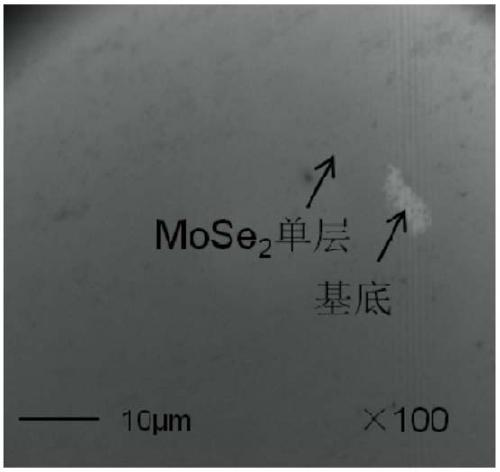
[0028] Embodiment 1 adopts Si / SiO 2 Synthesis of monolayer MoSe as a substrate 2 (1).

[0029] Synthesis of monolayer MoSe 2 The sample is made of molybdenum diselenide powder (99.9%), and the volume ratio of the gas is 95% inert gas Ar and 5% H 2 The mixed gas as carrier gas, with Si / SiO 2 Monolayer MoSe prepared by PVD method as substrate 2 . The only temperature zone of the high-temperature tube vacuum furnace is used not only as the area for melting and evaporating the molybdenum diselenide powder, but also as the area for the substrate to accept the sample deposition, so as to better control the temperature. The specific synthesis process is as follows: firstly, put quartz slices with length, width and height of 3cm, 2cm, and 1cm in a 10cm-long quartz boat, and then place Si / SiO 2×2×0.05cm 2 flakes and 0.1gMoSe 2The sample powder is placed on the quartz plate, while ensuring that the molybdenum diselenide powder is placed in front of the substrate, and finally they...

Embodiment 2

[0032] Embodiment 2 adopts Si / SiO 2 Synthesis of monolayer MoSe as a substrate 2 (2).

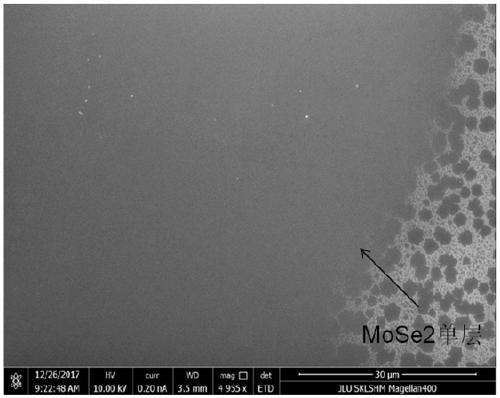
[0033] Si / SiO 2 As the substrate, monolayer MoSe was synthesized by PVD method 2 For the sample, when the synthesis process of Example 1 remains the same, the reaction conditions are set as follows: heating up to 960° C., holding time for 15 minutes, mixed gas flow rate of 25 sccm, and heating rate of 23° C. / min. Naturally cool to room temperature, and finally take out the quartz boat and the substrate for sample characterization. Si / SiO 2 MoSe prepared as substrate 2 The optical image of the monolayer sample is shown in Figure 5 As shown, it was found that there was a slight nodule phenomenon in the center of the sample, which was mainly caused by a slightly higher set temperature.

Embodiment 3

[0034] Example 3 is used as a comparative example. When the set temperature is higher than 970° C., a thick layer appears and the shape is irregular.

[0035] Si / SiO 2 As the substrate, monolayer MoSe was synthesized by PVD method 2 For the sample, when the synthesis process of Example 1 remains the same, the reaction conditions are set to be heated to 970° C., holding time is 15 minutes, mixed gas flow rate is 25 sccm, and the heating rate is 23° C. / min. Naturally cool to room temperature, and finally take out the quartz boat and the substrate for sample characterization. Si / SiO 2 MoSe prepared as substrate 2 The optical image of the monolayer sample is shown in Figure 6 As shown, it is found that the growth of the second layer begins on some monolayer samples, indicating that the high temperature may destroy the epitaxial growth of the monolayer.


PUM

PropertyMeasurementUnit
Sizeaaaaaaaaaa

Abstract

The invention discloses a method for synthesizing a single-layer transition metal chalcogenides, and belongs to the technical field of preparation of nano materials. The method comprises the followingsteps that molybdenum diselenide powder and tungsten diselenide powder are taken as raw materials and a gas mixture of inert gases Ar (95%) and H2 (5%) is taken as carrier gas; a PVD method is adopted to take an sole temperature region of a high-temperature tubular vacuum oven as both a powder melting and evaporating region and a region for a substrate to bear sample deposition; and a single-layer MoSe2 sample and a single-layer WSe2 sample are synthesized on a Si/SiO2 substrate and a sapphire substrate. The sample prepared by the invention is great in area, is relatively uniform, is good inquality and is high in repetitive rate. The preparation method has the advantages of simple operation, short reaction time,low cost, and no pollution on environment.

Description

technical field [0001] The invention belongs to the technical field of preparation of nanometer materials, in particular to a method for preparing single-layer transition metal chalcogenides. Background technique [0002] Transition metal dichalcogenides (TMDs) are two-dimensional materials with graphene-like structures formed by transition metal atoms and chalcogen atoms. They have unique physical properties, and they have potential wide application prospects in the design and development of new field effect transistors, light emitting diodes and photodetectors. Since monolayer materials with direct bandgap exhibit different optical and other properties from bulk materials with indirect bandgap, monolayer materials have attracted widespread attention. Among them, MoSe 2 and WSe 2 Transition metal chalcogenides, represented by single layers, show great application prospects in the fields of transistors, logic circuits, optoelectronic devices, sensors, and flexible devices...

Claims


Application Information

Patent Timeline
IPC IPC(8): C01B19/04
CPCC01B19/007C01P2004/20
Inventor 周强柳艳李芳菲
Owner JILIN UNIV
Why Eureka
Try Eureka