Thin-film solar cell and preparation method thereof

A technology of thin-film solar cells and transparent conductive films, applied in the field of solar cells, can solve the problems of low short-circuit current density of CdTe cells, and achieve the effects of suitable large-scale production, simple structure, and improvement of short-circuit current density

Inactive Publication Date: 2019-03-08
INST OF ELECTRICAL ENG CHINESE ACAD OF SCI
View PDF4 Cites 6 Cited by
  • Summary
  • Abstract
  • Description
  • Claims
  • Application Information

AI Technical Summary

Problems solved by technology

[0003] The current method for increasing the short-circuit current density of CdTe batteries is usually to use materials with larger band gaps as window layer materials, such as: using CdS:O / CdSe as window layer materials (Naba R.Paudel, Jonathan D.Poplawsky, Karren L. Moore, and Yanfa Yan, IEEE JOURNAL OF PHOTOVOLTAICS, VOL.5, NO.5, SEPTEMBER 2015, 1492~1496), using CdS:O as the window layer material (Jason M.Kephart, RussellM.Geisthardt, W.S.Sampath, Prog. Photovolt: Res.Appl.2015; 23:1484~1492), using CdS / ZnS as the window layer material (Isaiah O.Oladeji, Lee Chow, Christos S.Ferekides, VijayViswanathan, Zhiyong Zhao, Solar Energy Materials & Solar Cells 61 (2000) 203~211), but the CdTe batteries obtained by using these materials have a short-circuit current density of less than 30mA / cm 2 , the short-circuit current density of CdTe batteries is still low

Method used


Image

  • Thin-film solar cell and preparation method thereof
  • Thin-film solar cell and preparation method thereof

Examples


preparation example Construction

[0032] The present invention provides a method for preparing the thin film solar cell described in the above solution, which includes the following steps:

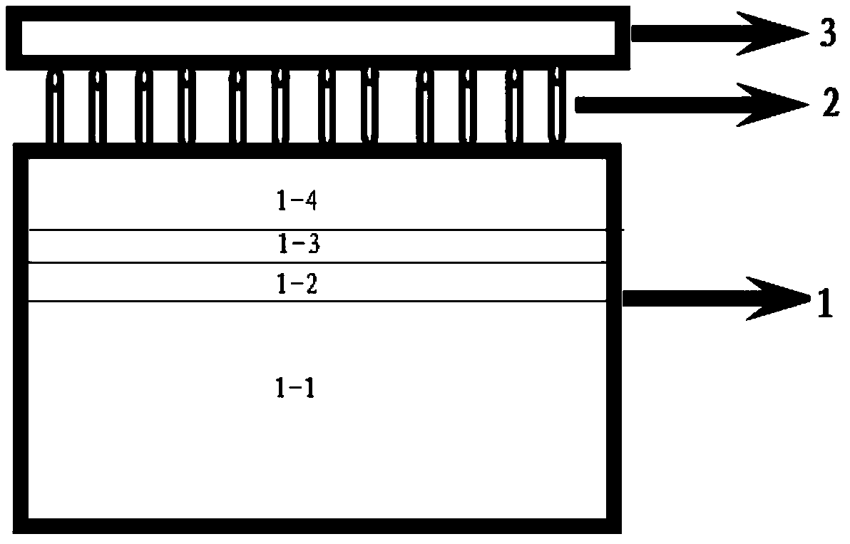
[0033] According to the structure of the thin film solar cell, a transparent conductive film, a window layer, a CdTe optical absorption layer, a quantum dot buffer layer and a conductive back electrode are sequentially prepared on a substrate.

[0034] The invention prepares a transparent conductive film on a substrate to obtain a transparent conductive film / substrate structure. In the present invention, the method for preparing the transparent conductive film on the substrate preferably includes a sol-gel method, a magnetron sputtering method or a chemical vapor deposition method.

[0035] In the present invention, the preparation parameters of the transparent conductive film prepared by the sol-gel method are not particularly limited, and preparation parameters well known to those skilled in the art may be used. In the embodim...

Embodiment 1

[0057] Using rigid glass as substrate, SnO is prepared on rigid glass by sol-gel method 2 : F(FTO) film, get SnO 2 :F(FTO) film / rigid glass structure; among them, SnO 2 : The preparation method of F(FTO) film is: take 50mLSnCl 2 And 50mLH 2 Dissolve O in 50mL of absolute ethanol, reflux at 80℃ for 4h, slowly add a mixture of water and ethanol in a 1:1 volume ratio; reflux at 80℃ for 3h, adjust the pH to 3; add 50mL formamide, add 50mLNH 4 F water solution, the prepared solution is allowed to stand for 24 hours; fix the cleaned substrate on the film spinning machine, spin the film at a speed of 2000r / min; then dry it in a vacuum drying oven at 100°C for 30 minutes, and then put it in the muffle In the furnace, slowly raise the temperature to 300°C and keep the temperature constant for 10 minutes; repeat the above film spinning process 4 times; finally treat at 600°C for 20 minutes; the SnO 2 : The thickness of the F(FTO) film is 200nm.

[0058] Using pulsed laser deposition method i...

Embodiment 2

[0064] Using flexible mica as the substrate material, ZnO:Al(AZO) film is prepared on flexible mica by magnetron sputtering method to obtain ZnO:Al(AZO) film / flexible mica structure; among them, ZnO:Al(AZO) film The preparation parameters are: the temperature of the flexible mica substrate is room temperature, the target base distance is 8cm, the carrier gas is argon, the pressure is 0.1Pa, and the sputtering power density is 2.78W / cm 2 The thickness of the ZnO: Al (AZO) film is 350 nm.

[0065] The CdS:O window layer was prepared on the ZnO:Al(AZO) film / flexible mica structure by magnetron sputtering, and the CdS:O window layer / ZnO:Al(AZO) film / flexible mica structure was obtained; among them, CdS:O The preparation parameters of the window layer are: ZnO:Al(AZO) film / flexible mica structure temperature is room temperature, target base distance is 13cm, carrier gas is argon / oxygen with a volume ratio of 56:1, pressure is 3Pa, sputtering The power density is 1.19W / cm 2 The thickne...


PUM


Abstract

The invention provides a thin-film solar cell and a preparation method thereof, and belongs to the field of solar cells. The thin-film solar cell comprises a substrate, a transparent conductive thin film, a window layer, a CdTe optical absorption layer, a quantum dot buffer layer and a conductive back electrode, which are sequentially laminated; and the quantum dot buffer layer comprises a SnSe quantum dot buffer layer or a Sb2Se3 quantum dot buffer layer. The SnSe quantum dot buffer layer or the Sb2Se3 quantum dot buffer layer serves as the quantum dot buffer layer; and the energy level of the SnSe quantum dot or the Sb2Se3 quantum dot is different from CdTe, so the light which cannot be absorbed by the CdTe can be absorbed, thereby improving the short-circuit current density. The experimental result of the embodiment shows that the short-circuit current density of the thin-film solar battery provided by the invention reaches 35. 64 mA / cm2; in addition, the thin-film solar cell provided by the invention is simple in structure and suitable for large-scale production.

Description

Technical field [0001] The invention belongs to the field of solar cells, and particularly relates to a thin film solar cell and a preparation method thereof. Background technique [0002] The structure of CdTe battery is usually: substrate / window layer / CdTe absorption layer / buffer layer / back electrode. Light passes through the substrate / window layer to reach the CdTe absorption layer. The material of the window layer is usually CdS, because the optical band gap of CdS is 2.4eV Before the light reaches the CdTe absorption layer, it will be absorbed by CdS in short wavelengths less than 510nm. The light absorbed by CdS does not contribute to the short-circuit current density of the CdTe battery. Therefore, the short-circuit current density of CdTe batteries is usually increased by reducing the thickness of CdS. However, as the thickness of the CdS decreases, the PN junction characteristics of the CdTe battery become worse, which reduces the open circuit voltage of the CdTe batter...

Claims


Application Information

Patent Timeline
Patent Type & Authority Applications(China)
IPC IPC(8): H01L31/032H01L31/0352H01L31/072H01L31/18B82Y40/00
CPCB82Y40/00H01L31/032H01L31/035218H01L31/072H01L31/18Y02E10/50Y02P70/50
Inventor 李辉古宏伟屈飞
Owner INST OF ELECTRICAL ENG CHINESE ACAD OF SCI
Why Eureka
Try Eureka