Pixel definition layer based on ink-jet printing and preparation method thereof

A pixel-defining layer, inkjet printing technology, applied in semiconductor/solid-state device manufacturing, electrical components, electrical solid-state devices, etc., can solve the problems of water vapor and oxygen permeability, high light transmittance, poor bottom spreading, etc., to improve stability , expand the range of choices, avoid the effect of influence

Inactive Publication Date: 2019-03-12
FUZHOU UNIVERSITY
View PDF5 Cites 5 Cited by
  • Summary
  • Abstract
  • Description
  • Claims
  • Application Information

AI Technical Summary

Problems solved by technology

[0004] Although the process is simple, the use of PI as the bank layer still has the following problems: the PI layer is porous and prone to residual solvents and functional molecules, water vapor and oxygen permeate, making the stability worse; the consistency and repeatability of the heating phase separation are poor, It is difficult to ensure the uniformity requirements of large-scale and large-scale

Method used


Image

  • Pixel definition layer based on ink-jet printing and preparation method thereof
  • Pixel definition layer based on ink-jet printing and preparation method thereof
  • Pixel definition layer based on ink-jet printing and preparation method thereof

Examples


Embodiment 1

[0029] A pixel-defining layer based on inkjet printing, the specific preparation method of which is:

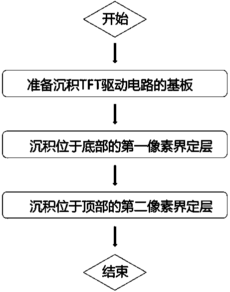
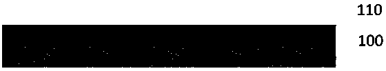
[0030] In the first step, a silicon substrate is provided, which is ultrasonically cleaned with acetone, alcohol, and deionized water in an atmospheric environment, dried, and deposited with TFT drive circuits and anodes, such as figure 2 ;

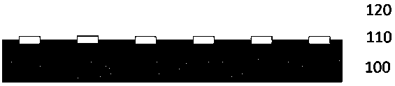
[0031] In the second step, use a fine metal mask to vapor-deposit a 100 nm-thick aluminum oxide on the substrate as the first pixel defining layer, such as image 3 ;

[0032] The third step is to dissolve polymethyl methacrylate (PMMA) and polystyrene (PS) at a certain stoichiometric ratio in tetrahydrofuran to make a polymer ink, and then prepare a patterned bank by inkjet printing, and let the tetrahydrofuran After the solvent evaporates, soak it in cyclohexane for a certain period of time, take it out, and let it dry naturally to obtain a hydrophobic second pixel defining layer with a thickness of 0.9 μm, as shown in Figure 4 . ...

Embodiment 2

[0034] A pixel-defining layer based on inkjet printing, the specific preparation method of which is:

[0035] In the first step, a silicon substrate is provided, which is ultrasonically cleaned with acetone, alcohol, and deionized water in an atmospheric environment, dried, and deposited with TFT drive circuits and anodes, such as figure 2 ;

[0036] In the second step, use a fine metal mask to sputter a layer of aluminum oxide with a thickness of 100 nm on the substrate as the first pixel defining layer, such as image 3 ;

[0037] The third step is to dissolve polymethyl methacrylate (PMMA) and polystyrene (PS) at a certain stoichiometric ratio in tetrahydrofuran to make a polymer ink, and then prepare a patterned bank by inkjet printing, and let the tetrahydrofuran After the solvent evaporates, soak it in cyclohexane for a certain period of time, take it out, and let it dry naturally to obtain a hydrophobic second pixel defining layer with a thickness of 0.9 μm, as shown...

Embodiment 3

[0039] A pixel-defining layer based on inkjet printing, the specific preparation method of which is:

[0040] In the first step, a silicon substrate is provided, which is ultrasonically cleaned with acetone, alcohol, and deionized water in an atmospheric environment, dried, and deposited with TFT drive circuits and anodes, such as figure 2 ;

[0041] In the second step, a 100-nm-thick aluminum oxide nanoparticle is deposited on the substrate as the first pixel-defining layer using a photolithography process, such as image 3 ;

[0042] The third step is to dissolve polymethyl methacrylate (PMMA) and polystyrene (PS) at a certain stoichiometric ratio in tetrahydrofuran to make a polymer ink, and then prepare a patterned bank by inkjet printing, and let the tetrahydrofuran After the solvent evaporates, soak it in cyclohexane for a certain period of time, take it out, and let it dry naturally to obtain a hydrophobic second pixel defining layer with a thickness of 0.9 μm, as sh...


PUM

PropertyMeasurementUnit
Thicknessaaaaaaaaaa
Thicknessaaaaaaaaaa
Thicknessaaaaaaaaaa

Abstract

The invention discloses a pixel definition layer based on ink-jet printing and a preparation method thereof. The method comprises the following three steps: preparing a substrate for depositing a TFTdrive circuit; depositing a first pixel definition layer located at the bottom; and depositing a second pixel definition layer located at the top, wherein the first pixel definition layer should be made of a material with excellent hydrophilic performance wettability, the second pixel definition layer should be made of the material with poor hydrophilic performance wettability, and the second pixel definition layer is a regular trapezoid structure; moreover, at least one of the first pixel definition layer and the second pixel definition layer is a lighttight material; at least one of the first pixel definition layer and the second pixel definition layer is an insulating material; the first pixel definition layer and the second definition layer both have ink solvent resistance; and the pixel definition layer can be realized through an etching or printing technology. With the pixel definition layer and the preparation method thereof, a selection range of a bank material is expanded greatly, influence on spreadability caused by boundary defects or structure is avoided effectively, stability is improved, meanwhile, a position of a pinning point can be regulated effectively, and fine control of evaporation, flowing and drying of ink is realized.

Description

technical field [0001] The invention belongs to the technical field of photoelectric device preparation, and in particular relates to a pixel defining layer based on inkjet printing and a preparation method thereof. Background technique [0002] Printed optoelectronic devices can effectively solve the shortcomings of high evaporation coating cost, poor substrate compatibility, and difficulty in achieving large areas. At the same time, they are green and environmentally friendly, and the process is simple, which is the future development direction. In the fabrication of pixelated photoelectric devices, a pixel definition layer (PDL), that is, a Bank, needs to be used. There are periodic recessed areas on the Bank layer as pixel pits for accommodating printing ink, and each pixel pit corresponds to a pixel unit. The currently widely used process for preparing printed electroluminescent devices is to accurately position the ink in each pixel pit by using the inkjet printing pr...

Claims


Application Information

Patent Timeline
IPC IPC(8): H01L51/56H01L27/32
CPCH10K59/122H10K71/135
Inventor 李福山刘洋胡海龙吕珊红马福民郭太良
Owner FUZHOU UNIVERSITY
Why Eureka
Try Eureka