A kind of inert metal n-type dopant and its application in organic electroluminescent devices
An inert metal and dopant technology, applied in the field of organic electroluminescent devices, can solve the problems of difficult long-term storage and use, unclear mechanism of action, unfavorable industrial production, etc., achieving convenient storage and use, and stable evaporation atmosphere. , beneficial to the effect of industrial production
- Summary
- Abstract
- Description
- Claims
- Application Information
AI Technical Summary
Problems solved by technology
Method used
Image
Examples
preparation example Construction
[0033] The preparation process of the organic electroluminescent device of the present invention is the same as that of the prior art, wherein the preparation method of the electron transport layer 08 is the conventional vacuum evaporation technology.
[0034] The vapor deposition rate of metal should be slower, be 0.1 angstrom / second, at this rate, the host material of electron transport layer and dopant material have the contact between compound and inert metal with coordination property more fully, make inert metal M and The ligand Ligand is more uniformly dispersed in the host material ETM, which is conducive to compounding.
Embodiment 1
[0036] The structure of a single-electron device:
[0037] ITO / Bphen(100nm) / Ag or Au: ETM: Ligand=(1:1:10, 1:1:5, 1:2:5, 1:2:10, 5-100nm) / Al;
[0038] First electrode layer 02 (anode ITO) / hole blocking layer 07 (Bphen) / electron transport layer 08 (x%M-Ligand-ETM) / second electrode layer 03 (cathode Al).
[0039] The host material ETM structure of the electron transport layer in this embodiment is as follows formula (a), and the doped inert metal is Ag or Au.
[0040]
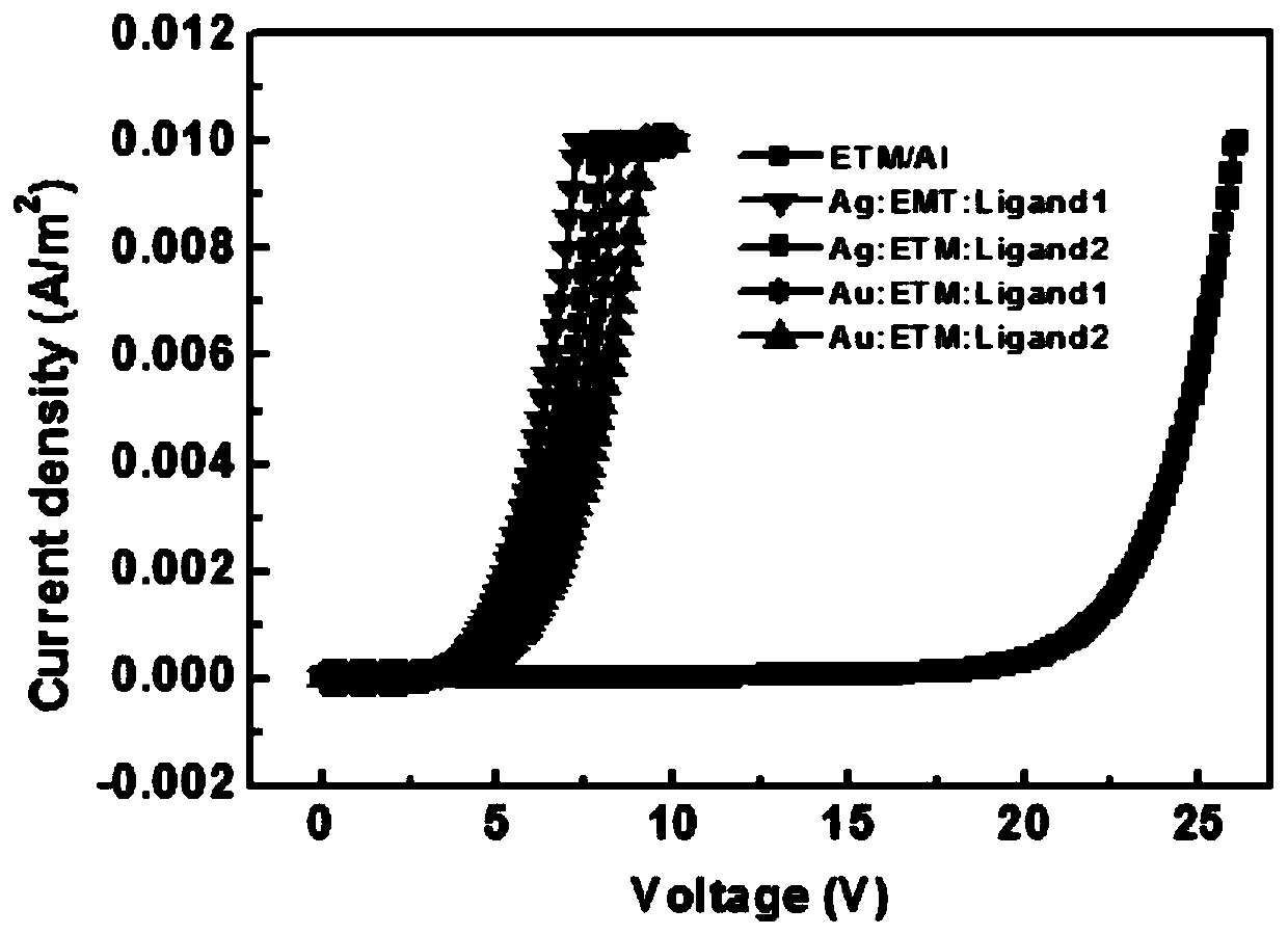
[0041] like figure 2 As shown, device 1 is the curve corresponding to ETM / Al, device 2 is the curve corresponding to Ag-ETM-Ligand1 / Al, device 3 is the curve corresponding to Ag-ETM-Ligand2 / Al, and device 4 is the curve corresponding to Au-ETM-Ligand1 / The curve corresponding to Al, device 5 is the curve corresponding to Au-ETM-Ligand2 / Al, the cathodes of devices 1-5 are all Al, where:
[0042] The electron transport layer 08 of the device 1 is the electron transport material shown in formula (a) (that is,...
Embodiment 2
[0049] Device structure:
[0050] ITO / HAT-CN(10nm) / NPB(30nm) / Alq 3 (30nm) / Bphen(20nm) / x%M-Ligand-ETM10nm / Ag;
[0051] The first electrode layer 02 (anode ITO), the hole injection layer 04 (HAT-CN), the hole transport layer 05 (NPB), the light emitting layer 06 (Alq 3 ), hole blocking layer 07 (Bphen), electron transport layer 08 (x%M-Ligand-ETM), second electrode layer 03 (cathode Ag).
[0052] The host material of the electron transport layer described in this embodiment is TPBI, which has the following structure:
[0053]
[0054] The host material, doped inert metal, and ligand compound of the electron transport layer described in this embodiment, as well as the composition ratio x% and doping ratio of the dopant are shown in Table 1 below, and are based on the existing Active metal doping is the control device.
[0055] Table 1 Material selection for each device
[0056] part number M Ligand M: Ligand ETM Mixing ratio vol% Device 6 Cu Fo...
PUM
 Abstract
Description
Claims
Application Information
 - R&D
- Intellectual Property
- Life Sciences
- Materials
- Tech Scout
- Unparalleled Data Quality
- Higher Quality Content
- 60% Fewer Hallucinations
Browse by: Latest US Patents, China's latest patents, Technical Efficacy Thesaurus, Application Domain, Technology Topic, Popular Technical Reports.
© 2025 PatSnap. All rights reserved.Legal|Privacy policy|Modern Slavery Act Transparency Statement|Sitemap|About US| Contact US: help@patsnap.com


