Cavity film bulk acoustic resonator capable of increasing q value and preparation method thereof
A bulk acoustic wave resonator, cavity film technology, applied in impedance networks, electrical components, etc., can solve the problems of increasing FBAR insertion loss, reducing energy conversion efficiency, reducing quality factor Q value, etc., to slow down overheating phenomenon, reduce Energy loss, thermal stress reduction effect
- Summary
- Abstract
- Description
- Claims
- Application Information
AI Technical Summary
Problems solved by technology
Method used
Image
Examples
Embodiment 1
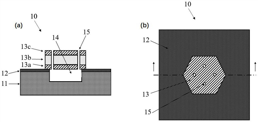
[0034] Such as figure 1 As shown, the cavity thin film bulk acoustic resonator 10 capable of improving the Q value provided by the first embodiment includes a substrate 11 , a SiC / Diamond thin film layer 12 and a piezoelectric oscillator stack 13 . The middle of the substrate 11 has a groove opening upwards. The SiC / Diamond thin film layer 12 is formed on the substrate, and a through opening corresponding to the groove is provided in the middle, and the size of the through opening is consistent with the groove. The piezoelectric oscillator stack part 13 is formed on the SiC / Diamond thin film layer 12 and is located directly above the through opening; the piezoelectric oscillator stack part 13 includes bottom electrode 13a, piezoelectric layer 13b, and top electrode 13c in order from bottom to top. The groove on the substrate 11 , the through opening on the SiC / Diamond thin film layer 12 , and the piezoelectric oscillator stack 13 together define a cavity 14 . Four release ho...
Embodiment 2
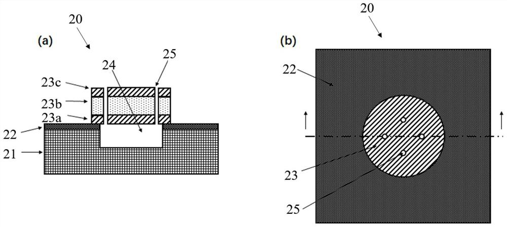
[0037] Such as figure 2 As shown, the cavity film bulk acoustic resonator 20 capable of improving the Q value provided by the second embodiment includes a substrate 21 , a SiC / Diamond film layer 22 and a piezoelectric oscillator stack 23 . The middle of the substrate 21 has a groove opening upwards. The SiC / Diamond thin film layer 22 is formed on the substrate, and a through opening corresponding to the groove is provided in the middle, and the size of the through opening is consistent with the groove. The piezoelectric oscillator stack part 23 is formed on the SiC / Diamond thin film layer 22 and is located directly above the through hole; the piezoelectric oscillator stack part 23 includes bottom electrode 23a, piezoelectric layer 23b, and top electrode 23c in order from bottom to top. The groove on the substrate 21 , the through hole on the SiC / Diamond thin film layer 22 , and the piezoelectric oscillator stack 23 together define a cavity 24 . Four release holes 25 are uni...
Embodiment 3
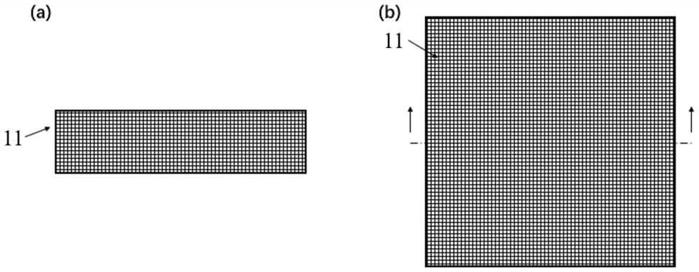
[0040]The third embodiment provides a method for preparing a cavity film bulk acoustic resonator that can improve the Q value. Here, the resonator in the first embodiment is taken as an example for illustration, and specifically includes the following steps:
[0041] 1) if image 3 As shown, a silicon substrate 11 is prepared;
[0042] 2) if Figure 4 As shown, a SiC / Diamond film layer 12 is grown on a silicon substrate 11;
[0043] 3) if Figure 5 As shown, a preset through hole 12a is etched on the SiC / Diamond film layer 12:
[0044] 4) if Figure 6 As shown, a preset groove 11a is etched on the silicon substrate 11;
[0045] 5) if Figure 7 As shown, a sacrificial layer A is deposited on the SiC / Diamond thin film layer 12 and in the groove 11a. The chemical properties of the material of the sacrificial layer A are different from those of the silicon substrate 11, ensuring that the substrate will not be affected during subsequent etching;
[0046] 6) If Figure 8 As ...
PUM
 Abstract
Description
Claims
Application Information


