Large-height-width-ratio microstructure transfer printing method

A high-aspect-ratio micro-, micro-nano structure technology is applied in the field of high-aspect-ratio microstructure transfer, which can solve the problem of difficult and high-aspect-ratio microstructure effective transfer, low success rate of ink transfer, and difficulty in realizing large height and width. Compared with the transfer of microstructures, it achieves the effect of low equipment environment requirements, wide range and simple manufacturing process.

Pending Publication Date: 2019-03-19
QINGDAO TECHNOLOGICAL UNIVERSITY
View PDF2 Cites 15 Cited by
  • Summary
  • Abstract
  • Description
  • Claims
  • Application Information

AI Technical Summary

Problems solved by technology

[0003] Compared with positive transfer printing, negative transfer printing and printing transfer printing, ink transfer printing has the advantages of lower cost, lower environmental requirements in the process and higher efficiency, and is more suitable for micro-nano devices with high yield requirements However, for the transfer printing of devices requiring large aspect ratio microstructures, the success rate of ink transfer is low or it is difficult to achieve the transfer printing of large aspe

Method used


Image

  • Large-height-width-ratio microstructure transfer printing method
  • Large-height-width-ratio microstructure transfer printing method

Examples


Embodiment 1

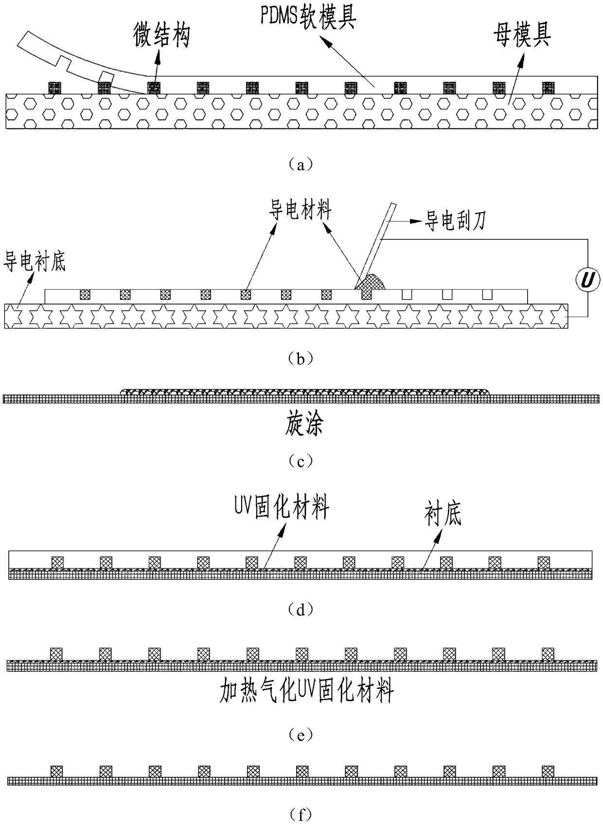
[0057] In this embodiment, the electric field-driven fused jet deposition 3D printing technology is used to manufacture the master mold required for micro-transfer printing. First, the microstructure in the master mold is transferred to the PDMS soft mold, wherein the microstructure is a PMMA wire grid structure; Fill the groove of the mold with conductive silver paste (containing glass powder) and pre-cure it; then select a common glass substrate and use UV-assisted transfer technology to transfer the conductive structure to the common glass substrate; finally sinter the conductive structure post-processing.

[0058] The specific process flow is: PDMS soft mold manufacturing, scrape coating of conductive materials, coating of UV curing materials, UV assisted transfer, and post-processing. Such as figure 1 (a) ~ (e) shown.

[0059] Specific steps are as follows:

[0060] Step 1: PDMS soft mold fabrication.

[0061] Step 1-1: Take the 3D printing master mold with a size of ...

Embodiment 2

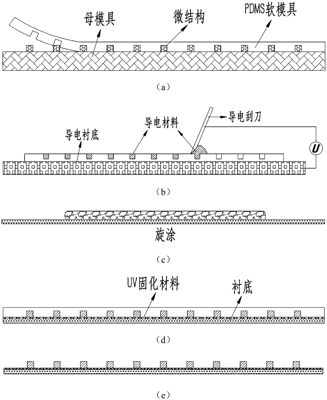
[0076] In this embodiment, the silicon mold manufactured by electron beam lithography is used as the master mold for micro-transfer printing. First, the microstructure on the silicon mold is transferred to the PDMS soft mold, wherein the microstructure is a grid structure; then, the microstructure on the PDMS soft mold The groove is filled with nano-silver conductive ink and pre-cured; after that, the PET film is selected as the target substrate, and the conductive structure is transferred to the PET film by UV-assisted transfer technology; finally, the conductive structure is post-processed.

[0077] The specific process flow is: PDMS soft mold manufacturing, scrape coating of conductive materials, coating of UV curing materials, UV assisted transfer, and post-processing. Such as figure 2 (a) ~ (e) shown.

[0078] Specific steps are as follows:

[0079] Step 1: PDMS soft mold fabrication.

[0080] Step 1-1: Take a 4-inch wafer silicon mold with a grid structure on it. The...

Embodiment 3

[0095] In this embodiment, the electric field-driven fused jet deposition 3D printing technology is used to manufacture the master mold required for micro-transfer printing. First, the microstructure is transferred to the PDMS soft mold, wherein the microstructure is a PCL grid structure; then, the groove of the PDMS soft mold The silver nanowire liquid is filled and pre-cured; after that, the PET film is selected as the substrate, and the conductive structure is transferred to the PET film by UV-assisted transfer technology; finally, the conductive structure is further post-processed.

[0096] The specific process flow is: PDMS soft mold manufacturing, scrape coating of conductive materials, coating of UV curing materials, UV assisted transfer, and post-processing. Such as figure 2 (a) ~ (e) shown.

[0097] Specific steps are as follows:

[0098] Step 1: PDMS soft mold fabrication.

[0099]Step 1-1: Take the 3D printing master mold with a size of 200mm×200mm, on which the...


PUM


Abstract

The invention relates to a large-aspect-ratio microstructure transfer printing method. According to the method, the template with the convex micro-nano structure is used as a mother mold, the liquid polydimethylsiloxane(PDMS) is poured to the mother mold, and heating is carried out to manufacture the PDMS soft die; a liquid conductive material is filled into the groove of the PDMS soft die throughan electric wetting auxiliary scraping and coating mode, and the conductive material is pre-cured at a certain temperature; the conductive material is transferred to the target substrate through a UVauxiliary transfer printing technology; the conductive structure on the target substrate is further processed to obtain the conductive structure which is good in consistency, high in precision and excellent in electric conduction performance.

Description

technical field [0001] The invention belongs to the technical field of micro-nano manufacturing, and in particular relates to a large aspect ratio microstructure transfer printing method. Background technique [0002] Micro-nano devices have broad application prospects in information, energy, medical, national defense and other fields, and are developing in the direction of intelligence and flexibility in recent years. The manufacturing technology and level of micro-nano directly determine the comprehensive performance of micro-components such as solar panels, micro-LEDs, flexible conductive films, sensors, biological devices, and wearable electronic devices. With the integration and development of multiple disciplines, more fields need to integrate micro-nano functional structural devices to meet different application requirements, thus posing new challenges to the manufacture of micro-nano structures. Micro-nano manufacturing technology requires low manufacturing cost, un...

Claims


Application Information

Patent Timeline
IPC IPC(8): B29C37/00B82Y40/00
CPCB29C37/0028B29C2037/0046B82Y40/00
Inventor 朱晓阳刘明杨兰红波李政豪张广明王飞
Owner QINGDAO TECHNOLOGICAL UNIVERSITY
Why Eureka
Try Eureka