Electroluminescent device based on ZnO film co-doped by erbium and fluorine and preparation method
An electroluminescent device and co-doping technology, which is applied in the field of optoelectronics, can solve the problems of complex device structure and harsh heat treatment conditions, and achieve the effect of simple and easy-to-operate preparation method
- Summary
- Abstract
- Description
- Claims
- Application Information
AI Technical Summary
Problems solved by technology
Method used
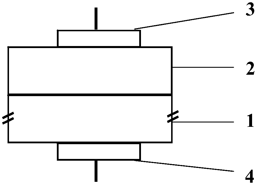
Image

Examples
Embodiment 1
[0041] (1) The size is 15×15mm 2 Epitaxial silicon epitaxial layer lightly doped with phosphorus (3-15Ω cm, thickness ~ 45μm) ) as a silicon substrate, after cleaning, put the silicon wafer in the radio frequency sputtering chamber, and use a vacuum pump to pump the pressure in the chamber to 5×10 -3 After Pa, pass high-purity O 2 gas and high-purity Ar gas (flow ratio O 2 :Ar=1:2) to air pressure 4Pa, use 1% ErF mixed with mole percentage 3 The ZnO ceramic target was sputtered to deposit the film, and the applied power was 120W; during the deposition process, the temperature of the silicon substrate was kept at 100°C, and the deposition time was 40min;
[0042] (2) Place the deposited film in O 2 Heat treatment at 700°C for 120 minutes in an air atmosphere, finally forming a ZnO film co-doped with Er and F, the thickness of the film is ~120nm, and the doping amount of Er is 1%, and the doping amount of F is 3% in atomic percentage;
[0043] (3) Deposit a transparent ITO ...
Embodiment 2
[0056] (1) The size is 15×15mm 2 Epitaxial silicon epitaxial layer lightly doped with phosphorus (3-15Ω cm, thickness ~ 45μm) ) as a silicon substrate, after cleaning, put the silicon wafer in the radio frequency sputtering chamber, and use a vacuum pump to pump the pressure in the chamber to 5×10 -3 After Pa, pass high-purity O 2 gas and high-purity Ar gas (flow ratio O 2 :Ar=1:2) to air pressure 4Pa, use 1% ErF mixed with mole percentage 3 The ZnO ceramic target was sputtered to deposit the film, and the applied power was 120W; during the deposition process, the temperature of the silicon substrate was kept at 100°C, and the deposition time was 40min;
[0057] (2) Place the deposited film in O 2 In gas atmosphere, heat treatment at 800°C for 120min, finally forming a ZnO film co-doped with Er and F, the thickness of the film is ~120nm, the doping amount of Er is 1%, and the doping amount of F is 3% in atomic percentage;
[0058] (3) Deposit a transparent ITO electrode w...
Embodiment 3
[0070] (1) The size is 15×15mm 2 Epitaxial silicon epitaxial layer lightly doped with phosphorus (3-15Ω cm, thickness ~45μm) ) as a silicon substrate, after cleaning, put the silicon wafer in the radio frequency sputtering chamber, and use a vacuum pump to pump the pressure in the chamber to 5×10 -3 After Pa, pass high-purity O 2 gas and high-purity Ar gas (flow ratio O 2 :Ar=1:2) to air pressure 4Pa, use 1% ErF mixed with mole percentage 3 , 2% Er 2 o 3 The ZnO ceramic target was sputtered to deposit the film, and the applied power was 120W; during the deposition process, the temperature of the silicon substrate was kept at 100°C, and the deposition time was 40min;
[0071] (2) Place the deposited film in O 2 In the atmosphere, heat treatment at 700°C for 120 minutes, finally forming a ZnO film co-doped with Er and F, the thickness of the film is ~120nm, the doping amount of Er is 5% atomic ratio, and the doping amount of F is 3% atomic ratio;
[0072] (3) Deposit a tran...
PUM
| Property | Measurement | Unit |
|---|---|---|
| Thickness | aaaaa | aaaaa |
| Thickness | aaaaa | aaaaa |
| Resistivity | aaaaa | aaaaa |
Abstract
Description
Claims
Application Information
 - R&D
- Intellectual Property
- Life Sciences
- Materials
- Tech Scout
- Unparalleled Data Quality
- Higher Quality Content
- 60% Fewer Hallucinations
Browse by: Latest US Patents, China's latest patents, Technical Efficacy Thesaurus, Application Domain, Technology Topic, Popular Technical Reports.
© 2025 PatSnap. All rights reserved.Legal|Privacy policy|Modern Slavery Act Transparency Statement|Sitemap|About US| Contact US: help@patsnap.com