

Preparation method of carbon nanometer film/nano-micrometer network composite film
A technology of carbon nano-film and network compounding, applied in gaseous chemical plating, metal material coating process, coating, etc., can solve the problems of incomplete coordination of neighbors, high equipment requirements, high decomposition temperature, etc., to reduce time and expand The effect of applying the foreground
- Summary
- Abstract
- Description
- Claims
- Application Information
AI Technical Summary
Problems solved by technology
Method used
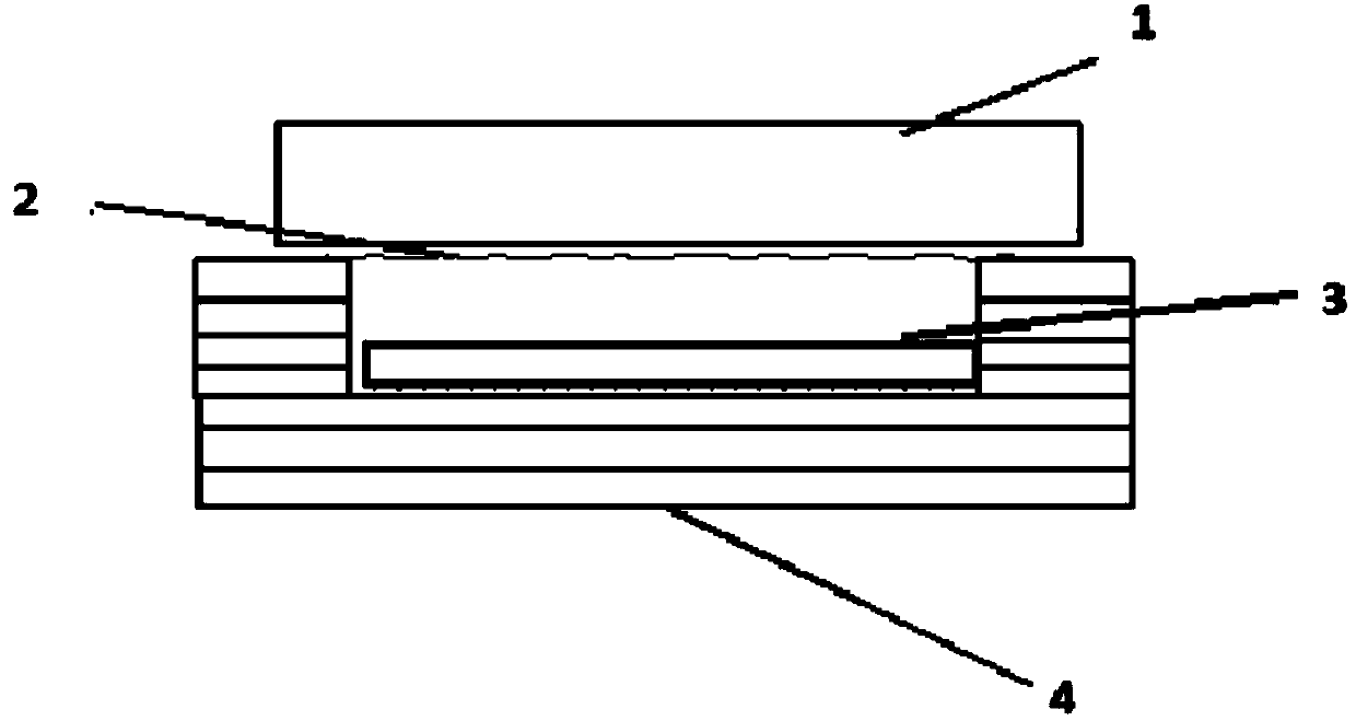
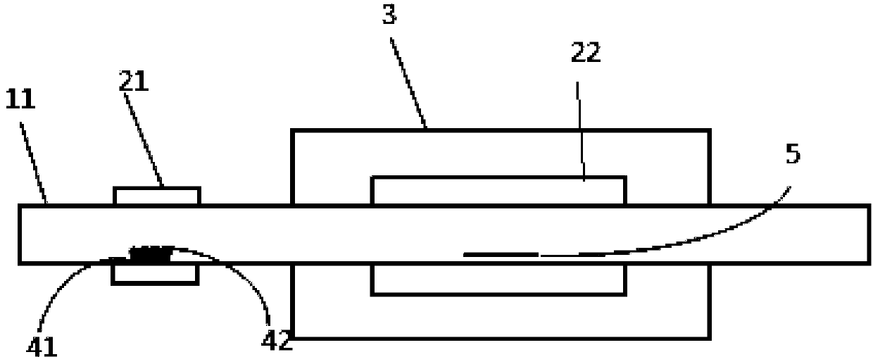
Image

Examples
Embodiment 1
[0159] Step 1: After the purchased high-purity copper foil is electrochemically polished, wash off the residual electrolyte on the high-purity copper foil with deionized water, and wash it in acetone, alcohol, and deionized water 2-3 times, each time 10 Minutes, dry the copper foil with nitrogen.
[0160] Step 2: Put the copper foil into a tube furnace, and anneal at high temperature under the protection of hydrogen and argon. After the annealing is completed, cool with the furnace and take out the copper foil to obtain the first substrate. In this embodiment, the flow rate of hydrogen gas is preferably 30 sccm, the flow rate of argon gas is 300 sccm, the annealing temperature is 1020° C., and the annealing time is 1 h.
[0161] Step 3: spread the self-supporting carbon nanotube film prepared by the CVD method on the first substrate, and infiltrate it with alcohol. In this embodiment, the thickness of the carbon nanotube film is 10 nm, and the pores range from 100 nm to 1000 n...
Embodiment 2
[0169] Step 1-3 is identical with step 1-3 in embodiment 1;
[0170] Step 4: Spin-coat the PMMA solution on the first substrate with the carbon nanotube film attached, and place it at one end of the quartz tube (non-growth temperature zone). In this embodiment, the spin coating speed is 4000r / min;
[0171] Step 5: Introduce cleaning gas into the reaction chamber until the air in the chamber is completely removed; in this embodiment, 500 sccm high-purity argon is preferably used as the cleaning gas, and the cleaning time is 10 minutes.
[0172] Step 6: After the cleaning is completed, adjust the flow meter and raise the temperature to T1 under the atmosphere of hydrogen and argon. After the temperature is stabilized, the carbon nanotube film / first substrate spin-coated with PMMA is moved to the growth temperature zone of the tube furnace, and the temperature is rapidly raised to T1, and the growth time is t1. In this embodiment, the flow rate of hydrogen gas is 30 sccm, the f...
Embodiment 3
[0176] The copper foil in Example 1 is replaced by a copper-nickel alloy, and the preparation method of the copper-nickel alloy is as follows: the high-purity copper foil after the annealing treatment is used as the cathode (25 μm in this embodiment), and the high-purity nickel plate is used as the anode. Electroplating 2-5μm nickel film on copper foil, the electroplating solution used is a mixture of 250g / L nickel sulfate hexahydrate, 50g / L boric acid, 50g / L nickel chloride hexahydrate and 0.1g / L sodium lauryl sulfate solution, the electroplating current is set to 0.01A / cm2, and the electroplating time is set to 5 minutes to 30 minutes. After electroplating, the copper / nickel foil plate is heat-treated at 1000° C. for 2 hours in an atmosphere of argon and hydrogen to form a copper-nickel alloy.
[0177] Subsequent steps are the same as in Example 1.
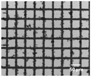
[0178] Example results: the graphene / carbon nanotube composite film is finally obtained, and the graphene / carbon nanotube com...
PUM
| Property | Measurement | Unit |
|---|---|---|
| Thickness | aaaaa | aaaaa |
| Concentration | aaaaa | aaaaa |
| Pore size | aaaaa | aaaaa |
Abstract
Description
Claims
Application Information