Microring resonator with improved coupled zone and manufacturing method thereof

A micro-ring resonator and coupling region technology, applied in the field of integrated optics, can solve the problems that the accuracy of ordinary lithography technology is difficult to meet the requirements, the cost of lithography technology is high, and the surface cannot be flattened, and the thickness is more controllable. Easy, consistent results

Active Publication Date: 2019-03-29
UNIV OF ELECTRONICS SCI & TECH OF CHINA
View PDF8 Cites 9 Cited by
  • Summary
  • Abstract
  • Description
  • Claims
  • Application Information

AI Technical Summary

Problems solved by technology

[0003] At present, although microring resonators have been realized in different materials such as SOI (Silicon-On-Insulator, silicon on an insulating substrate), organic polymers, and lithium niobate, their iconic parameters such as loss and modulation depth , free spectral range, quality factor, etc., there is still a lot of room for improvement
In addition, most microring resonators use a horizontal coupling structure. In terms of coupling spacing, for devices using horizontal coupling, the general coupling spacing is about 200nm. From the perspective of process implementation, the coupling spacing of horizontal coupling is narrow. The precision is difficult to meet the requirements, and the cost of more advanced lithography technology is too high
The resonator using the vertical coupling structure is also faced with the problem that the surface of each layer cannot be flat on the multi-layer structure, which will aggravate the problem of device loss, which offsets the advantages brought by the use of the vertical coupling structure, and also faces difficulties in application.

Method used


Image

  • Microring resonator with improved coupled zone and manufacturing method thereof
  • Microring resonator with improved coupled zone and manufacturing method thereof
  • Microring resonator with improved coupled zone and manufacturing method thereof

Examples


Embodiment Construction

[0047] In order to make the purpose, technical solution and advantages of the present invention clearer, the microring resonator with improved coupling region and its manufacturing method provided by the present invention will be described in detail below in conjunction with specific embodiments and with reference to the accompanying drawings. .

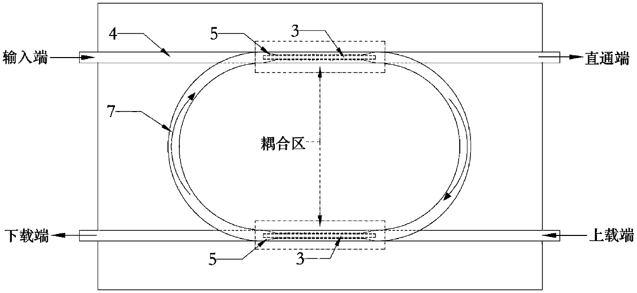
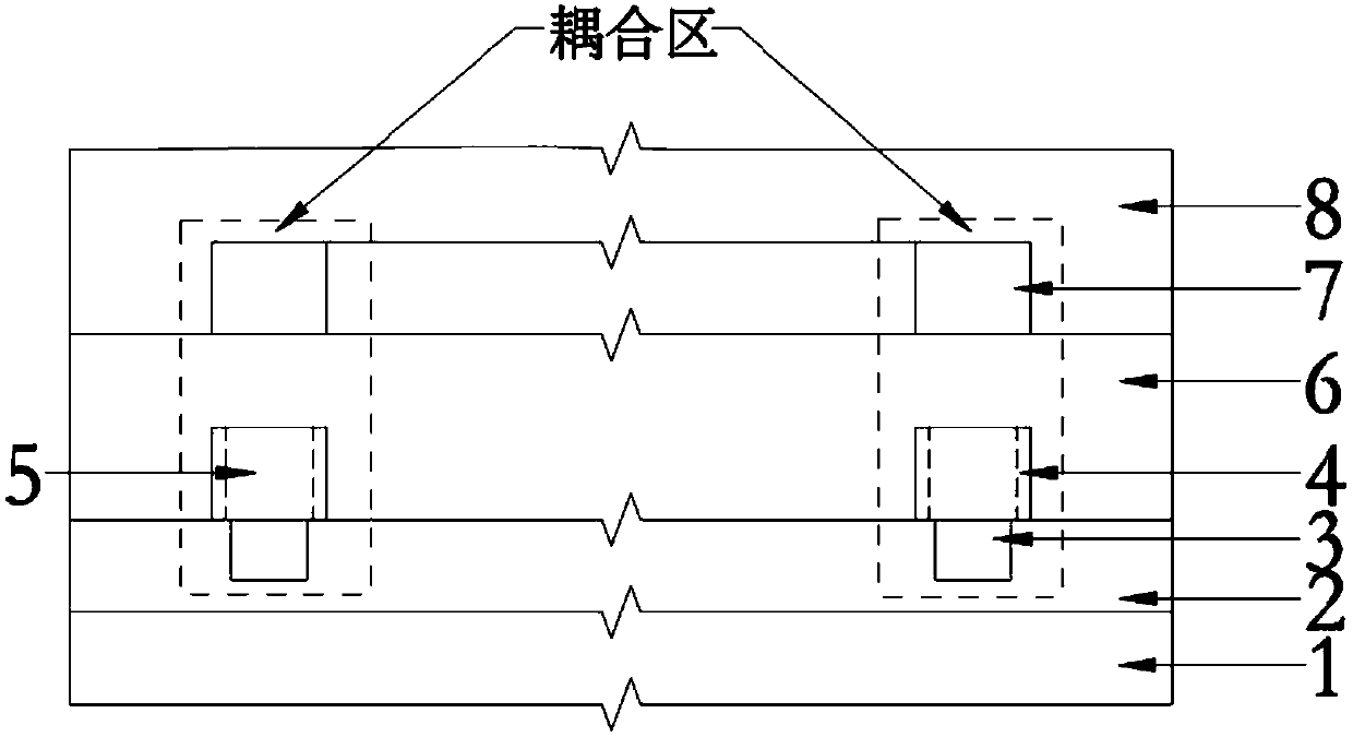
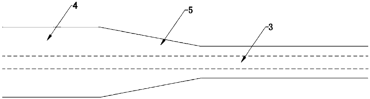
[0048] figure 1 is a top view of the microring resonator structure of the present invention. Such as figure 1 As shown, the present invention is a microring resonator adopting a vertical coupling structure, and its basic symmetrical structure includes a straight waveguide 4, a racetrack waveguide 7, a buried groove 3, and a trapezoidal structure 5, and light is coupled into from the input end of the straight waveguide 4. The device is transmitted along the straight waveguide 4 , a part of the light field is coupled into the racetrack waveguide 7 in the trapezoidal structure 5 of the coupling region, and a part is output along the s...


PUM


Abstract

The invention provides a microring resonator with an improved coupled zone and a manufacturing method thereof, and belongs to the field of integrated optics. The device comprises a substrate 1, a bonding layer 2, a straight waveguide 4, a dielectric layer 6 and a racetrack type waveguide 7; the bonding layer 2 is disposed on the substrate 1, the dielectric layer 6 is disposed on the bonding layer2, the straight waveguide 4 is disposed in the dielectric layer 6, a straight channel portion of the racetrack type waveguide 7 is located directly above the straight waveguide 4. The device is characterized by further comprising a burying groove 3, which is formed in the bonding layer 2 in a coupling area, and located directly under the straight waveguide 4; and the refractive index of the burying groove 3 is smaller than the refractive index of the substrate 1. According to the microring resonator with the improved coupled zone and the manufacturing method thereof, by adopting the burying groove structure, leakage loss of a light field during transmission can be reduced, and transferring from the light field to other media can be promoted, thereby improving coupling efficiency, and an advantage of promoting change from a multimode mode to mode reduction in a ridge waveguide can be obtained.

Description

technical field [0001] The invention belongs to the field of integrated optics, and in particular relates to a device structure of a microring resonant cavity with an improved coupling region and a related manufacturing method. Background technique [0002] Integrated optics is one of the frontiers in the field of optics and optoelectronics. Its main research contents include collimation, deflection, filtering, space radiation, optical oscillation, conduction, amplification, modulation of light waves in thin film materials and related thin films. Nonlinear optical effects of materials, etc. In recent years, with the development of micromachining technologies such as ion beam implantation, direct bonding, and focused ion beam etching, the deepening of optoelectronics research, and the discovery of materials with various optical properties, integrated optics is gradually becoming mature. In 1969, Marcatili[1] and others proposed a microring resonator and simulated a bandpass ...

Claims


Application Information

Patent Timeline
Patent Type & Authority Applications(China)
IPC IPC(8): G02B6/12
CPCG02B6/12G02B6/12004G02B6/12007G02B2006/12142
Inventor 帅垚乔石珺高琴吴传贵罗文博王韬张万里
Owner UNIV OF ELECTRONICS SCI & TECH OF CHINA
Why Eureka
Try Eureka