Hydrogenated amorphous silicon film preparation method

A technology for the preparation of hydrogenated amorphous silicon and thin films, which is applied in the manufacture of semiconductor/solid-state devices, electrical components, circuits, etc., can solve the problem of insignificant improvement of passivation effect, and achieves the optimization of interface quality, the improvement of minority carrier life, and the improvement of efficiency. Effect

Active Publication Date: 2019-03-29
NANCHANG UNIV
View PDF12 Cites 4 Cited by
  • Summary
  • Abstract
  • Description
  • Claims
  • Application Information

AI Technical Summary

Problems solved by technology

[0006] The purpose of the present invention is to provide a method for preparing a hydrogenated amorphous silicon film, which effectively solves the technical problem that the passivation effect of the a-Si:H film is not significantly improved in the prior art

Method used


Image

  • Hydrogenated amorphous silicon film preparation method
  • Hydrogenated amorphous silicon film preparation method
  • Hydrogenated amorphous silicon film preparation method

Examples


Embodiment Construction

[0024] The essence of the present invention will be further described below in conjunction with the accompanying drawings and examples, but the content of the present invention is not limited thereto.

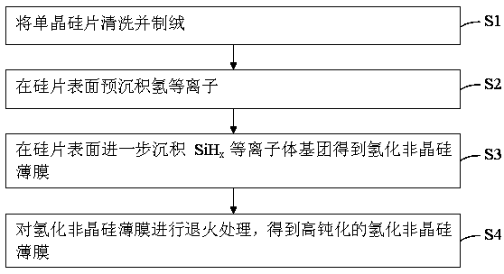
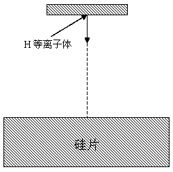
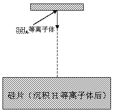
[0025] Such as figure 1 Shown is the hydrogenated amorphous silicon thin film preparation method provided by the present invention. It can be seen from the figure that the preparation method includes: S1 cleaning and texturing the single crystal silicon wafer; S2 pre-depositing hydrogen plasma on the surface of the silicon wafer; S3 further deposits SiH on the surface of the silicon wafer x Plasma group to obtain a hydrogenated amorphous silicon film, where x=1 or 2 or 3; S4 annealing the hydrogenated amorphous silicon film to obtain a highly passivated hydrogenated amorphous silicon film.

[0026] In this preparation method, the cleaned and textured silicon wafer is placed in a PECVD chamber, the incident kinetic energy of H plasma is controlled by PECVD technology, the silic...


PUM

PropertyMeasurementUnit
thicknessaaaaaaaaaa

Abstract

The invention discloses a hydrogenated amorphous silicon film preparation method. The method comprises steps that S1, a single crystal silicon chip is cleaned and texturied; S2, hydrogen plasmas are pre-deposited on the surface of the silicon chip; S3, a SiHx plasma group is further deposited on the surface of the silicon chip to obtain a hydrogenated amorphous silicon film, and x=1 or 2 Or 3; andS4, the hydrogenated amorphous silicon film is annealed to obtain a highly-passivated hydrogenated amorphous silicon film. The method is advantaged in that through combination of early stage treatment of H plasma deposition for the silicon chip and annealing treatment of the a-Si:H film, interface area defect density is effectively reduced, the a-Si / c:Si interface quality is optimized, and efficiency of an HIT battery is further improved.

Description

technical field [0001] The invention relates to the technical field of renewable energy, in particular to a method for preparing a hydrogenated amorphous silicon film. Background technique [0002] With the globalization of the economy, China's economy and industry have developed rapidly, and the demand for energy has increased sharply. China and the world are facing an energy crisis. The development of non-polluting, renewable, and low-cost new energy has become an important part of today's world energy development. The inevitable trend and mainstream. Solar energy is the conversion of sunlight energy into electrical energy. Solar photovoltaic power generation is considered to be an effective way to solve the global energy crisis and an important part of future energy production. [0003] At present, the photoelectric conversion efficiency of amorphous silicon / crystalline silicon heterojunction solar cells (Hetero-junction with Intrinsic Thin-layer, hereinafter referred to...

Claims


Application Information

Patent Timeline
Patent Type & Authority Applications(China)
IPC IPC(8): H01L21/02
CPCH01L21/02H01L21/02521H01L21/0262Y02P70/50
Inventor 周耐根罗耀榕周浪黄海宾
Owner NANCHANG UNIV
Why Eureka
Try Eureka