Manufacturing method of magnetic radom access memory unit array and peripheral circuit connecting wires

A random access memory and cell array technology, applied in the manufacture/processing of electromagnetic devices, circuits, electrical components, etc., can solve problems such as small size openings, MRAM device pollution, damage diffusion barriers, etc., to achieve complexity and production costs Effects of reduction, device electrical performance and yield improvement, and magnetic/electrical performance improvement

Inactive Publication Date: 2019-03-29
SHANGHAI CIYU INFORMATION TECH
View PDF2 Cites 7 Cited by
  • Summary
  • Abstract
  • Description
  • Claims
  • Application Information

AI Technical Summary

Problems solved by technology

However, since the size of the MTJ structural unit is smaller than that of the VIA x (x>=1) The size of the top opening is small. When etching the magnetic tunnel junction and its bottom electrode, in order to completely isolate the MTJ units, over-etching must be carried out. In the over-etching, the magnetic tunnel junction is not blocked. and its bottom electrode covered copper VIA x (x>=1) area will be partially etched, and also damage its diffusion barrier layer (Ta / TaN), which will form copper VIA x (x>=1) to the diffusion channel of the low-k dielectric outside it, Cu atom will be diffused in the low-k dielectric, and this is bound to affect the electrical performance of MRAM, such as: time-dependent dielectric breakdown (TDDB , Time Dependent DielectricBreakdown) and electron mobility (EM, Electron Mobility), etc., causing damage
[0007] In addition, during the over-etching process of the magnetic tunnel junction and its bottom electrode, due to ion bombardment (IonBombardment), copper atoms and their forming compounds will be sputtered to the sidewall of the magnetic tunnel junction and the etched low-k material surface, thereby contaminating the entire MRAM device

Method used


Image

  • Manufacturing method of magnetic radom access memory unit array and peripheral circuit connecting wires
  • Manufacturing method of magnetic radom access memory unit array and peripheral circuit connecting wires
  • Manufacturing method of magnetic radom access memory unit array and peripheral circuit connecting wires

Examples


Embodiment example 1

[0063] Implementation case 1: two single damascene (SD, Single Damascene) processes, the steps are as follows:

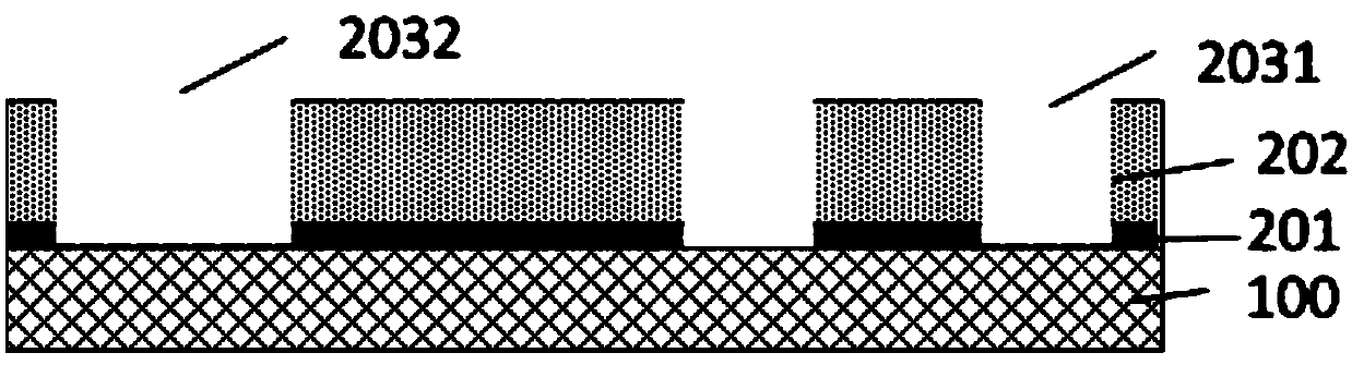
[0064] Step 3.1.1: On the magnetic tunnel junction dielectric capping layer (II) 401, deposit the top electrode via dielectric 402, and finally, use a planarization process to grind the top electrode via (TEV) dielectric 402, as shown in Figure 3(a) shown; the top electrode via (TEV) dielectric 402 is SiO 2 , SiON or low-k and other materials, the thickness of which is 120nm ~ 400nm.

[0065] Step 3.1.2: Graphically define and use an etching process to form top electrode through holes (TEV) 4031 and top electrode through holes 4032; in the logic area, connect them to the bottom electrode contact metal layer 301; in the storage area, connect them to To the top hard mask layer 303, typically, a cleaning process is used to remove the polymer after etching, as shown in FIG. 3(b).

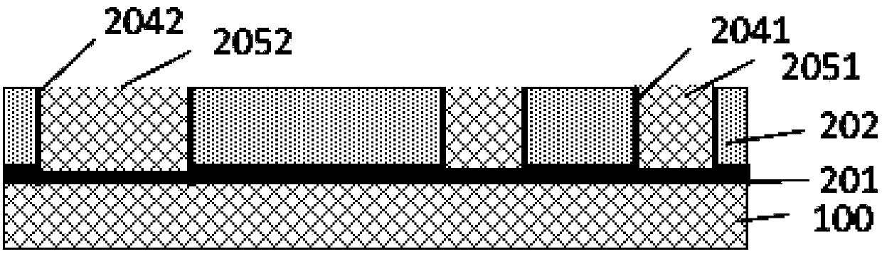
[0066] Step 3.1.3: filling metal to form top electrode via hole filling 4051 and top el...

Embodiment example 2

[0068] Implementation case 2: a dual damascene (DD, Dual Damascene) process, such as Figure 4 shown; the steps are as follows:

[0069] Step 3.2.1: On the magnetic tunnel junction dielectric capping layer (II) 401, deposit the top electrode via hole dielectric 402, and then use a planarization process to grind the top electrode via (TEV) dielectric 402 flat; the top electrode via (TEV) ) Dielectric 402 is SiO 2 , SiON or low-k and other materials, the thickness of which is 120nm ~ 400nm; finally, deposit metal wiring (M x+1 ) The thickness of dielectric 502 is 50nm~300nm, and its material is SiO 2 , SiON or low-k, etc., usually before deposition, an etch stop layer 501 with a thickness of tens of nanometers is deposited, and its material is SiN, SiC or SiCN.

[0070] Step 3.2.2: Graphically define and use an etching process to form the top electrode through hole (TEV) and the metal wiring groove connecting the logic area and the storage area. In the logic area, connect the...


PUM


Abstract

The invention provides a manufacturing method of a magnetic radom access memory unit array and peripheral circuit connecting wires. The manufacturing method comprises the steps of: (1) providing a surface-polished CMOS substrate with metal connecting wires, forming bottom electrode vias in the substrate, then filling the bottom electrode vias with non-copper metal and grinding the surface of the metal to be flat; (2) making memory region bottom electrode contact manufacturing a magnetic tunnel junction array on the bottom electrode vias in a memory region, and making logic region bottom electrode contact on the bottom electrode vias in a logic region; (3) and forming top electrode vias, and manufacturing metal connecting wires realizing connection with a logic/memory unit. Thus, a bottom electrode contact metal film and a magnetic tunnel junction multilayer film can be deposited at one time, thereby being conductive to improving the magnetic/electrical performance of the magnetic radomaccess memory, simplifying the complexity of the process and reducing the manufacturing cost.

Description

technical field [0001] The invention relates to a manufacturing method of a magnetic random access memory (MRAM) unit array and peripheral circuit wiring, and belongs to the technical field of magnetic random access memory (MRAM, Magnetic Radom Access Memory) manufacturing. Background technique [0002] In recent years, MRAM using Magnetic Tunnel Junction (MTJ) is considered to be the future solid-state non-volatile memory, which has the characteristics of high-speed reading and writing, large capacity and low energy consumption. Ferromagnetic MTJ is usually a sandwich structure, which has a magnetic memory layer, which can change the magnetization direction to record different data; an insulating tunnel barrier layer in the middle; a magnetic reference layer, located on the other side of the tunnel barrier layer, which The direction of magnetization remains unchanged. [0003] In order to record information in this magnetoresistive element, it is suggested to use a writing...

Claims


Application Information

Patent Timeline
Patent Type & Authority Applications(China)
IPC IPC(8): H01L43/12H01L27/22
CPCH10B61/00H10N50/01
Inventor 肖荣福张云森叶力郭一民陈峻
Owner SHANGHAI CIYU INFORMATION TECH
Why Eureka
Try Eureka