N-type polysilicon crystal and manufacturing method thereof, and N-type polysilicon wafer
A manufacturing method, polysilicon technology, applied in crystal growth, polycrystalline material growth, final product manufacturing, etc., can solve the problems of low conversion efficiency and low production yield of P-type polysilicon, and achieve high quality, excellent conversion efficiency, high resistance evenly distributed effect
- Summary
- Abstract
- Description
- Claims
- Application Information
AI Technical Summary
Problems solved by technology
Method used
Image

Examples
preparation example Construction
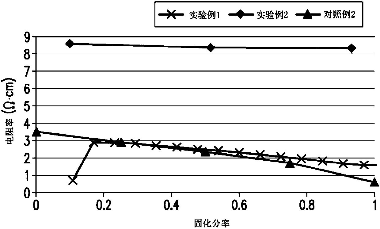
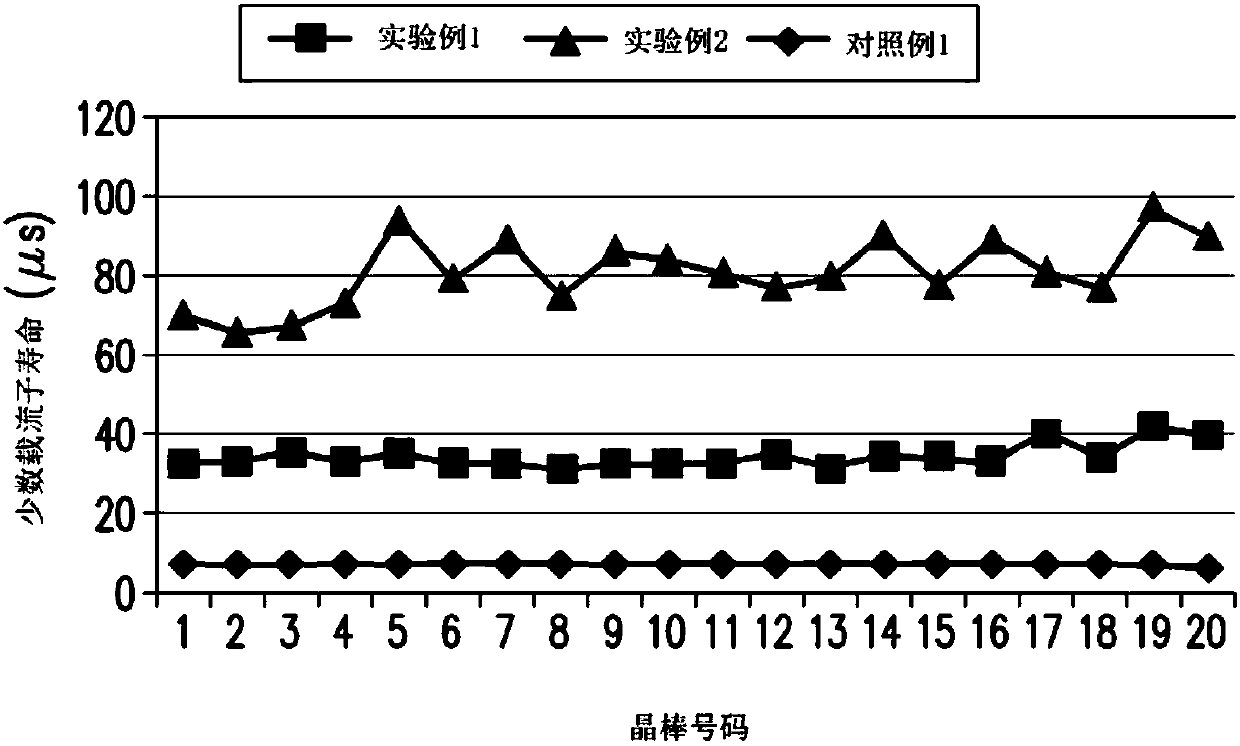
[0054] According to the preparation method of the first embodiment, the grown N-type polysilicon crystal grown by DSS has a resistivity slope and a defect area ratio slope. When the unit of the abscissa axis is curing fraction and the unit of ordinate axis is ohm·centimeter (Ω·cm), the resistivity slope is 0 to -1.8 when the curing fraction is 0.25˜0.8. When the unit of the horizontal axis of the coordinate is the solidification fraction and the unit of the vertical axis of the coordinate is the proportion of defect area (%), the slope of the proportion of the defect area when the solidification fraction is 0.4-0.8 is less than 2.5.
[0055] In this paper, "solidified fraction" refers to the ratio of the height of the solidified part in the crystal growth direction V to the total height of the silicon crystal during the solidification process of the N-type polysilicon crystal. The earlier the solidification fraction of the crystal is, the smaller the solidification fraction is...
experiment example 1
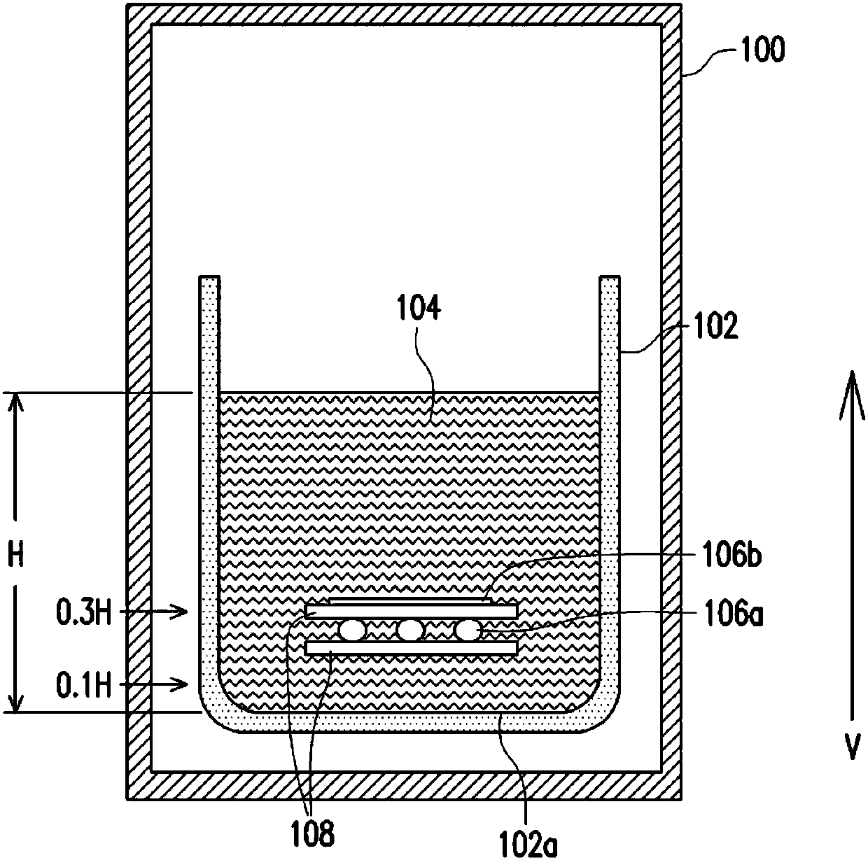
[0061] Silicon materials and dopants (gallium particles and phosphorus doped sheets) such as figure 1 Placed in a graphite crucible, the position of the dopant is set in the area of 0.25H from the bottom of the crucible, wherein the doping amount of gallium is 1.953ppma, and the doping amount of phosphorus is 0.180ppma. The atomic ratio of gallium and phosphorus is 10.85.
[0062] Raise the temperature above 1414°C without the cover to allow the silicon to start melting. When the temperature rises to 1500°C ~ 1570°C, the silicon material will completely melt into a silicon melt, and then grow crystals through temperature control. The initial temperature of crystal growth is set at 1385°C to 1430°C, and the final temperature is set at 1385°C to 1400°C. After the crystal growth is completed, the annealing and cooling processes are completed in sequence, and what is grown is an n-type polysilicon crystal.
experiment example 2
[0064] The same crystal growth steps and dopant placement as in Experimental Example 1 were adopted, but the doping amounts of gallium and phosphorus were changed to 0.632ppma and 0.044ppma, respectively. The atomic ratio of gallium and phosphorus is 14.36. What is grown is an n-type polysilicon crystal.
PUM
| Property | Measurement | Unit |
|---|---|---|
| particle diameter | aaaaa | aaaaa |
| electrical resistivity | aaaaa | aaaaa |
| electrical resistivity | aaaaa | aaaaa |
Abstract
Description
Claims
Application Information
 - R&D
- Intellectual Property
- Life Sciences
- Materials
- Tech Scout
- Unparalleled Data Quality
- Higher Quality Content
- 60% Fewer Hallucinations
Browse by: Latest US Patents, China's latest patents, Technical Efficacy Thesaurus, Application Domain, Technology Topic, Popular Technical Reports.
© 2025 PatSnap. All rights reserved.Legal|Privacy policy|Modern Slavery Act Transparency Statement|Sitemap|About US| Contact US: help@patsnap.com