Manufacturing method of flexible tft substrate and manufacturing method of flexible oled panel

A manufacturing method and flexible substrate technology, applied in semiconductor/solid-state device manufacturing, vacuum evaporation plating, coating, etc., can solve the problems of SD metal layer 200 fracture, affecting TFT properties, and yield decline, so as to reduce heat, Effect of preventing outgassing and improving properties

Active Publication Date: 2020-09-08
TCL CHINA STAR OPTOELECTRONICS TECH CO LTD
View PDF5 Cites 0 Cited by
  • Summary
  • Abstract
  • Description
  • Claims
  • Application Information

AI Technical Summary

Problems solved by technology

[0005] In the manufacturing process of the LTPS-TFT backplane of the traditional flexible OLED panel, such as figure 1 Shown is a schematic structural diagram of an existing flexible OLED panel. In order to enhance the bendability of the flexible TFT backplane, a deep hole (deep hole, DH) 100 will be etched in the bending area (bending area), and then the DH100 The ODH material (organic deep hole material) is filled in the center; however, when the source drain (SD) is fabricated subsequently, the SD metal layer 200 needs to be deposited by physical vapor deposition (Physical Vapor Deposition, PVD), because the sputtering chamber The indoor temperature is relatively high, about 220°C-230°C, and the sputtering power is about 40-50kw. During the process of slowly depositing the SD metal layer 200, the heat will slowly accumulate, and the accumulated heat will make the ODH in the lower DH100 Outgassing occurs in the material, which eventually causes the SD metal layer 200 above it to break or even fall off, which seriously affects the properties of the TFT and reduces the yield.

Method used


Image

  • Manufacturing method of flexible tft substrate and manufacturing method of flexible oled panel
  • Manufacturing method of flexible tft substrate and manufacturing method of flexible oled panel
  • Manufacturing method of flexible tft substrate and manufacturing method of flexible oled panel

Examples


Embodiment Construction

[0033] In order to further illustrate the technical means adopted by the present invention and its effects, the following describes in detail in conjunction with preferred embodiments of the present invention and accompanying drawings.

[0034] see figure 2 , the present invention firstly provides a kind of manufacturing method of flexible TFT substrate, comprises the following steps:

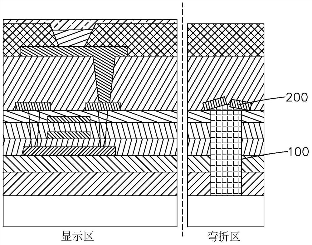
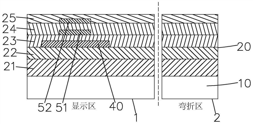
[0035] Step S1, such as image 3 As shown, a flexible substrate 10 is provided, and a barrier layer 21 and a buffer layer 22 of inorganic non-metallic materials are sequentially deposited on the flexible substrate 10, a polysilicon active layer 40 is formed on the buffer layer 22, and a polysilicon active layer 40 is formed on the buffer layer. 22 and the polysilicon active layer 40 are deposited to form a first gate insulating layer 23 of inorganic non-metallic material, deposited and patterned on the first gate insulating layer 23 to form a first gate metal layer 51, in the The second gate...


PUM


Abstract

Provided in the present invention are a manufacturing method for a flexible TFT substrate and a manufacturing method for a flexible OLED panel. The manufacturing method for a flexible TFT substrate according to the present invention uses a physical vapor deposition (PVD) method to deposit and form a source-drain metal layer by means of sputtering corresponding elements. In the process of depositing the source-drain metal layer by means of PVD, the inner temperature of a sputtering chamber is 90-100°C, and the sputtering power is 20-30 kW. Thus, the inner temperature and the sputtering power of the sputtering chamber used when depositing a source-drain metal layer by PVD are less than those of the prior art, thereby reducing heat of an organic photoresist block in a deep hole for bending accumulated in the process of depositing the source-drain metal layer, which can prevent outgassing of the organic photoresist block in the deep hole for bending, reduce the risk of breakage and detachment of the source-drain metal layer at this position, and significantly improve the properties of the flexible TFT substrate and product yields.

Description

technical field [0001] The invention relates to the field of display technology, in particular to a method for manufacturing a flexible TFT substrate and a method for manufacturing a flexible OLED panel. Background technique [0002] In the field of display technology, flat panel display devices such as Liquid Crystal Display (LCD) and Active Matrix Organic Light-Emitting Diode (AMOLED) display have thin body, high image quality, Many advantages such as power saving and no radiation have been widely used, such as mobile phones, personal digital assistants (PDAs), digital cameras, computer screens or notebook screens, etc. [0003] Thin Film Transistor (Thin Film Transistor, TFT) array (Array) substrate is the main component of current LCD devices and AMOLED devices, directly related to the development direction of high-performance flat panel display devices, used to provide drive circuits for displays, usually equipped with several A gate scanning line and several data line...

Claims


Application Information

Patent Timeline
Patent Type & Authority Patents(China)
IPC IPC(8): H01L27/12H01L21/285H01L21/77C23C14/34C23C14/18C23C14/04
CPCC23C14/04C23C14/18C23C14/34H01L21/2855H01L27/1248H01L27/1259
Inventor 张卜芳李松杉
Owner TCL CHINA STAR OPTOELECTRONICS TECH CO LTD
Why Eureka
Try Eureka