Infrared detector based on hybrid plasmon resonance enhancement
A plasmon resonance and infrared detector technology, applied in the field of infrared detectors, can solve the problems of high cost of photodetector preparation, difficulty in modulation of absorption band, low light absorption, etc., and achieve the effect of easy preparation, high responsivity, and enhanced absorption
- Summary
- Abstract
- Description
- Claims
- Application Information
AI Technical Summary
Problems solved by technology
Method used
Image
Examples
Embodiment 1
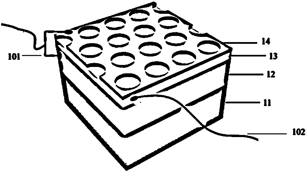
[0044] to combine figure 1 As shown, the infrared detector based on hybrid plasmon resonance enhancement provided in this embodiment uses a substrate 11 (the material is silicon / silicon dioxide, the thickness of silicon dioxide is 100~300 nm, and the thickness of silicon is 200 nm. ~600 mm), the bottom metal film 12 (made of gold, with a thickness of 100 nm), the middle semiconductor layer 13 (made of zinc oxide, with a thickness of 50 nm), and the top layer of metal nanopores are sequentially arranged on the substrate 11 from bottom to top. The array layer 14 (made of gold with a thickness of 40 nm) also includes electrode wires 101 drawn out from the top and bottom metal film layers, and electrode wires 102 drawn out from the middle semiconductor layer, and the wires are respectively used as output ports of the detector . Through numerical simulation calculations, when the center-to-center distance between two adjacent nanoholes in the top metal layer is 600 nm and the dia...
Embodiment 2
[0054] Its structure see figure 1 , the same as in Example 1, except that the distance between the centers of two adjacent holes of the top metal nanohole array is changed from 600 nm in Example 1 to 1000 nm, and the middle semiconductor layer is changed from 50 nm zinc oxide in Example 1. 30nm titanium dioxide. By changing the process parameters of the ion etching system, the diameters of polystyrene spheres were reduced from 1000 nm to 820 nm, 770 nm, 700 nm and 600 nm, respectively.
[0055] Among them, the top-view SEM image of the device prepared when the diameter of the polystyrene sphere is reduced to 770 nm is shown in the attached Figure 6 shown.
[0056] The reflection spectrum curve 71 with a nanopore diameter of 820 nm, the reflection spectrum curve 72 with a nanopore diameter of 770 nm, the reflection spectrum curve 73 with a nanopore diameter of 700 nm, and the reflection spectrum curve with a nanopore diameter of 600 nm prepared in this example Reflectance ...
PUM
 Abstract
Description
Claims
Application Information


