Infrared detector based on hybrid plasmon resonance enhancement

A technology of plasmon resonance and infrared detectors, which is applied in the field of infrared detectors, can solve the problems of low light absorption, difficulty in modulation of absorption band, high cost of optical detector preparation, etc., and achieve the effect of high responsivity detection

Active Publication Date: 2022-04-01
SUZHOU UNIV
View PDF3 Cites 0 Cited by
  • Summary
  • Abstract
  • Description
  • Claims
  • Application Information

AI Technical Summary

Problems solved by technology

[0006] In order to solve the problems of relatively high preparation cost, low light absorption and difficult modulation of absorption bands in the prior art, the present invention adopts the following technical solution: an infrared detector based on hybrid plasmon resonance enhancement , the infrared detector is a composite layer structure, and the bottom metal film layer, the middle semiconductor layer and the top metal micro-nanohole array layer are arranged sequentially on the substrate from bottom to top; wherein the bottom metal film layer and the top metal micro-nanohole array layer The array layers are connected by wires, and the electrode wires are respectively drawn out from the bottom metal film layer and the middle semiconductor layer

Method used


Image

  • Infrared detector based on hybrid plasmon resonance enhancement
  • Infrared detector based on hybrid plasmon resonance enhancement
  • Infrared detector based on hybrid plasmon resonance enhancement

Examples


Embodiment 1

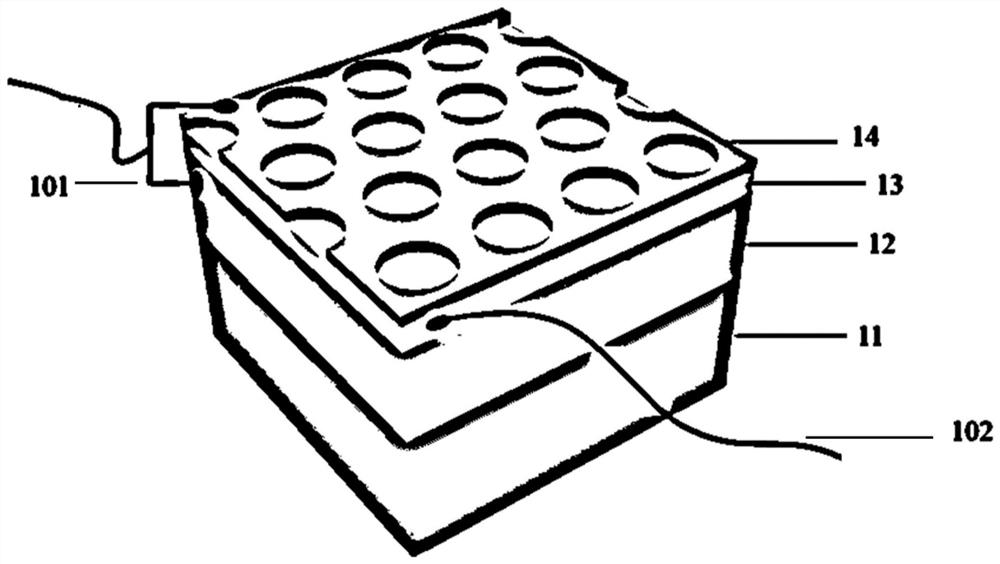
[0044] to combine figure 1 As shown, the infrared detector based on hybrid plasmon resonance enhancement provided in this embodiment adopts a substrate 11 (the material is silicon / silicon dioxide, the thickness of silicon dioxide is 100-300 nm, and the thickness of silicon is 200-200 nm. 600 μm), the bottom metal film layer 12 (made of gold, with a thickness of 100 nm), the middle semiconductor layer 13 (made of zinc oxide, with a thickness of 50 nm), and the top metal nanohole array layer 14 are sequentially arranged on the substrate 11 from bottom to top. (Material is gold, thickness is 40nm), also includes the electrode wire 101 that top and bottom two metal film layers lead out, and the electrode wire 102 that is drawn out by middle semiconductor layer, described wire is used as the output port of detector respectively. Through numerical simulation calculations, when the center-to-center distance between two adjacent nanoholes in the top metal layer is 600nm and the diame...

Embodiment 2

[0054] Its structure see figure 1 , the same as in Example 1, except that the center-to-center distance of two adjacent holes of the top metal nanohole array is changed from 600nm in Example 1 to 1000nm, and the middle semiconductor layer is changed from 50nm zinc oxide in Example 1 to 30nm. Titanium dioxide. By changing the process parameters of the ion etching system, the diameter of polystyrene spheres was reduced from 1000nm to 820nm, 770nm, 700nm and 600nm respectively.

[0055] Among them, the top-view SEM image of the device prepared when the diameter of the polystyrene sphere is reduced to 770nm is shown in the attached Image 6 shown.

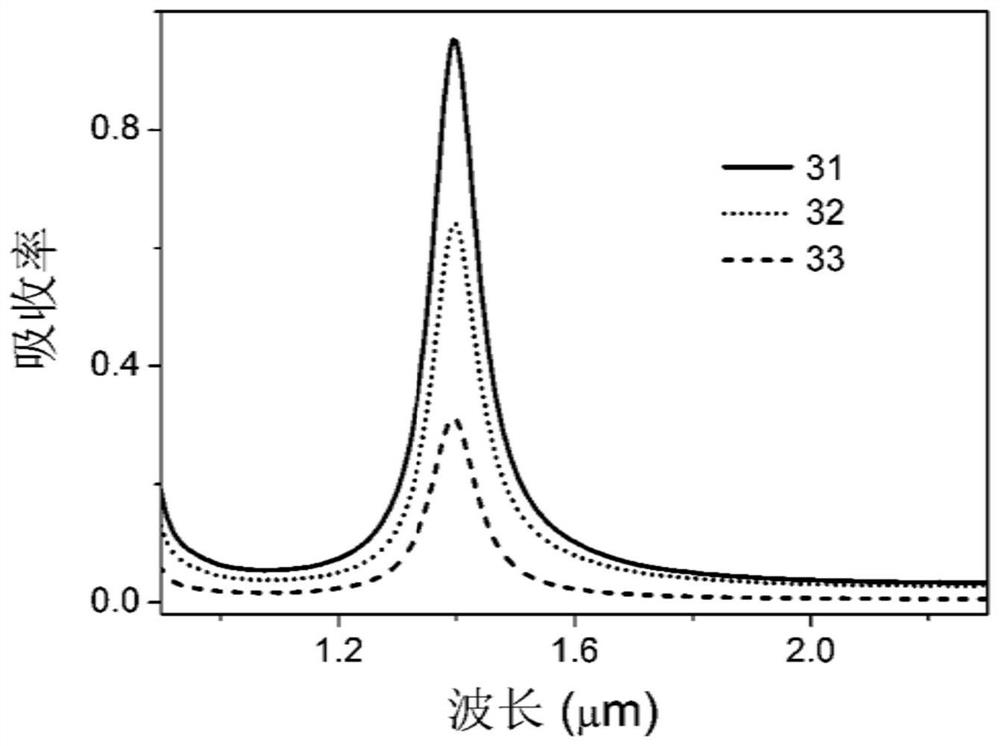
[0056] The reflection spectrum curve 71 with a nanopore diameter of 820nm, the reflection spectrum curve 72 with a nanopore diameter of 770nm, the reflection spectrum curve 73 with a nanopore diameter of 700nm, and the reflection spectrum curve 74 with a nanopore diameter of 600nm prepared in this embodiment , as attached Figure ...


PUM

PropertyMeasurementUnit
thicknessaaaaaaaaaa
thicknessaaaaaaaaaa
thicknessaaaaaaaaaa

Abstract

The invention belongs to the field of photoelectric detection and sensing technology. In order to solve the problems of high preparation cost, low light absorption and difficult modulation of absorption bands in the prior art, a photodetector based on hybrid plasmon resonance is proposed. Enhanced infrared detector, using metal micro-nano hole array layer / semiconductor thin film / metal thin film composite structure to build a thermal electron infrared detector based on metal absorption; by exciting the local plasmon resonance of the top metal micro-nano hole array, the bottom metal film layer Surface plasmons, and the hybrid plasmon resonance formed by coupling the two to greatly increase the absorption of incident light by the metal, and inject the hot carriers generated by the absorption of light by the upper and lower metal layers into the intermediate semiconductor layer, so as to obtain considerable light responsivity; by adjusting the period and diameter of the micro-nano hole in the top layer, the thickness and refractive index of the middle semiconductor layer, the tunable spectral absorption from near-infrared to mid-infrared can be realized.

Description

technical field [0001] The invention belongs to the technical field of photoelectric detection and sensing, and relates to an infrared detector. Background technique [0002] The development of infrared detectors is the forerunner of the development of infrared technology, and the technical level of a country's infrared detectors represents the level of its infrared technology development. In recent decades, infrared technology has been used in a wide range of applications, such as reconnaissance, night vision, guidance, meteorology, landforms, environmental monitoring, remote sensing, thermal imaging, and spectroscopy. With the broadening of application fields, people have higher demands on the range of infrared detection bands. In order to promote the development of infrared technology, developed countries such as Europe and the United States have taken the lead in launching the seamless spectrum band detection plan, and have made important progress in the detection of lo...

Claims


Application Information

Patent Timeline
Patent Type & Authority Patents(China)
IPC IPC(8): H01L31/108H01L31/18
CPCH01L31/108H01L31/18Y02P70/50
Inventor 吴绍龙丁浩徐玉亭眭博闻张程秦琳玲李孝峰
Owner SUZHOU UNIV
Why Eureka
Try Eureka