Metallic oxide thin film transistor and preparation method thereof

A technology of oxide thin film and oxide semiconductor, which is applied in the field of electronics, can solve the problems of limited application field of working voltage, inability to apply implantable devices, inability to use flexible materials, etc., achieve high capacitance value, low cost, and improve electrical performance Effect

Inactive Publication Date: 2019-05-17
XIAN JIAOTONG LIVERPOOL UNIV
View PDF3 Cites 4 Cited by
  • Summary
  • Abstract
  • Description
  • Claims
  • Application Information

AI Technical Summary

Problems solved by technology

[0004] (a) In order to form a functional ZnO semiconductor film, the annealing temperature needs to reach at least 350°C, making it impossible to apply to flexible materials such as Pi,
[0005] (b) The use of SiO2 insulating layer in the traditional process leads to the working voltage is usually above ten volts
The higher working voltage limits its wider application fields,
[0006] (c) The traditional solution preparation process often uses highly toxic 2-mercaptoethanol solution as the precursor solution, which pollutes the environment and cannot be applied to implantable devices

Method used


Image

  • Metallic oxide thin film transistor and preparation method thereof
  • Metallic oxide thin film transistor and preparation method thereof
  • Metallic oxide thin film transistor and preparation method thereof

Examples


Embodiment 2

[0048] The manufacturing process of the bottom-gate top-contact water-liquid method low-voltage high-performance metal oxide thin film transistor of the present invention comprises the following steps:

[0049] a) cleaning treatment of insulating substrate;

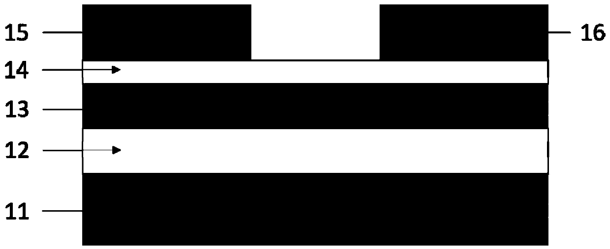
[0050] b) Depositing the gate electrode by thermal evaporation (12)

[0051] c) Surface water treatment

[0052] d) Spin-coating annealing in aqueous solution to obtain gate insulating layer

[0053] e) Spin-coating and annealing in aqueous solution to obtain a metal oxide semiconductor layer

[0054] f) Obtaining the pattern of the gate insulating layer and the double-layer metal oxide semiconductor layer by photolithographic wet etching.

[0055] g) The insulating substrate cleaning treatment process of the step a) of depositing the source and drain electrodes by the lift-off process includes the following steps:

[0056] 1. Ultrasonic cleaning of flexible substrate-Pi film / quartz (11) with acetone for 10 minutes; ...


PUM

PropertyMeasurementUnit
thicknessaaaaaaaaaa

Abstract

The invention belongs to the field of thin film transistors, and relates to a metallic oxide thin film transistor and a preparation method thereof. The thin film transistor includes an insulating substrate, a gate electrode, a gate insulating layer, a metallic oxide semiconductor layer, a source electrode and a drain electrode. The insulating substrate is located at the bottommost layer of an organic thin film transistor, the gate electrode, the gate insulating layer and the metallic oxide semiconductor layer are sequentially stacked on the insulating substrate from bottom to top, and the source electrode and the drain electrode are separately located above the metallic oxide semiconductor layer. According to the preparation method of the metallic oxide semiconductor thin film, the performance and carrier mobility of a ZnO-based thin film transistor prepared by an aqueous solution method in the prior art are improved by adding an alkali metal compound to a polymeric precursor solution,the preparation process is simple, the production cost is low, and the whole process temperature is controlled within 300 DEG C.

Description

technical field [0001] The invention relates to the field of electronic technology, in particular to an electronic device, in particular to a low-voltage high-performance metal oxide thin film transistor and a preparation method thereof. Background technique [0002] With the advancement of modern display technology, people's demand for high-performance thin film transistors is increasing. Metal oxide thin film transistors prepared by the solution method have attracted much attention in recent years. They have high mobility and transmittance, but also have the advantages of low cost, low temperature preparation, easy application in flexible materials and large-area integration. Therefore, metal oxide thin film transistors prepared by solution method have become a research hotspot in recent years. [0003] ZnO-based metal oxide thin film transistors are currently mainly prepared by high-vacuum methods such as atomic layer deposition, magnetron sputtering, and pulsed laser de...

Claims


Application Information

Patent Timeline
Patent Type & Authority Applications(China)
IPC IPC(8): H01L21/34H01L29/786H01L29/227
Inventor 刘启晗赵春赵策洲杨莉王琦男
Owner XIAN JIAOTONG LIVERPOOL UNIV
Why Eureka
Try Eureka