Multi-layer metal net grid electromagnetic shielding optical window employing femtosecond laser etching and fabrication method thereof
An electromagnetic shielding, multi-layer metal technology, applied in the direction of magnetic/electric field shielding, electrical components, etc., can solve the problem that the metal grid cannot be in the low-frequency electromagnetic band, etc., and achieve high visible and infrared light transmittance, long service life, high transparency Overrate effect
- Summary
- Abstract
- Description
- Claims
- Application Information
AI Technical Summary
Problems solved by technology
Method used
Image
Examples
Embodiment 1
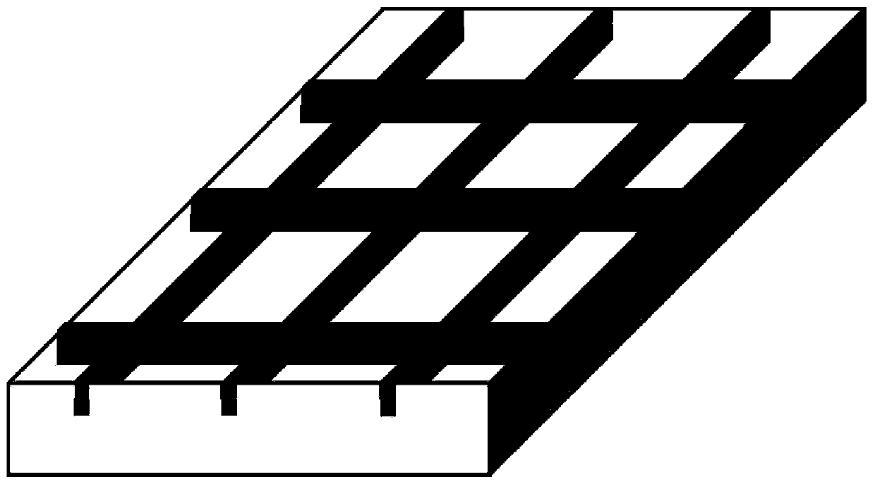
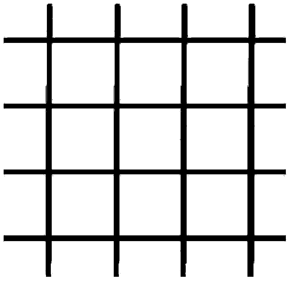
[0038] Embodiment 1: Utilize the electromagnetic shielding light window of the double-layer square metal mesh grid of femtosecond laser etching, such as figure 1As shown, the electromagnetic shielding optical window is composed of a metal grid layer 1 composed of gold, a metal grid layer 2 composed of nickel, a transparent dielectric substrate quartz glass 3, a metal grid layer 4 composed of nickel, and a metal grid layer composed of gold. Metal grid layer 5 constitutes. The period of the metal grid is set to 160um, the line width is set to 8um, the thickness of the nickel layer is 500nm, and the thickness of the gold layer is 1um. The thickness of the transparent medium substrate is set to h, and the value range of h is set to 2mm-12mm.
[0039] The equipment method of the electromagnetic shielding light window of the double-layer square metal mesh grid etched by femtosecond laser is as follows Figure 8 Shown: Place the prepared quartz glass sheet in a mixed solution of ac...
Embodiment 2
[0040] Embodiment 2: Utilize the electromagnetic shielding light window of the three-layer grid metal mesh grid of femtosecond laser etching, such as Figure 7 As shown, the electromagnetic shielding optical window described above is composed of a metal grid layer 1 composed of gold, a metal grid layer 2 composed of nickel, a first layer of transparent dielectric substrate quartz glass 3, a metal grid layer 4 composed of gold, and a metal grid layer 4 composed of nickel. The formed metal grid layer 5, the second transparent dielectric substrate quartz glass 6, the metal grid layer 7 made of nickel and the metal grid layer 8 made of gold are composed. The period of the metal grid is set to 160um, the line width is set to 8um, the thickness of the nickel layer is 500nm, and the thickness of the gold layer is 1um.
[0041] The equipment method of the electromagnetic shielding light window of the double-layer square metal mesh grid etched by femtosecond laser is as follows Figur...
PUM
| Property | Measurement | Unit |
|---|---|---|
| electrical conductivity | aaaaa | aaaaa |
| thickness | aaaaa | aaaaa |
| infrared transmittance | aaaaa | aaaaa |
Abstract
Description
Claims
Application Information


