Manufacturing method based on photocuring 3D printing technology and used for circuit board

A 3D printing and manufacturing method technology, applied in the directions of additive manufacturing, processing manufacturing, manufacturing tools, etc., can solve the problem of relying on expensive injection molding equipment and molds, not suitable for manufacturing small and medium-scale customized products, etc., to reduce production equipment and molds. The effect of investment, shortened production cycle and short process flow

Inactive Publication Date: 2019-05-21
SOUTHEAST UNIV
View PDF3 Cites 8 Cited by
  • Summary
  • Abstract
  • Description
  • Claims
  • Application Information

AI Technical Summary

Problems solved by technology

However, the molding interconnection equipment technology based on the injection molding process needs to rely on expensive injection molding equipment and molds, which is only suitable for mass production, not suitable for the manufacture of small and medium-sized customized products

Method used


Image

  • Manufacturing method based on photocuring 3D printing technology and used for circuit board
  • Manufacturing method based on photocuring 3D printing technology and used for circuit board
  • Manufacturing method based on photocuring 3D printing technology and used for circuit board

Examples


example 1

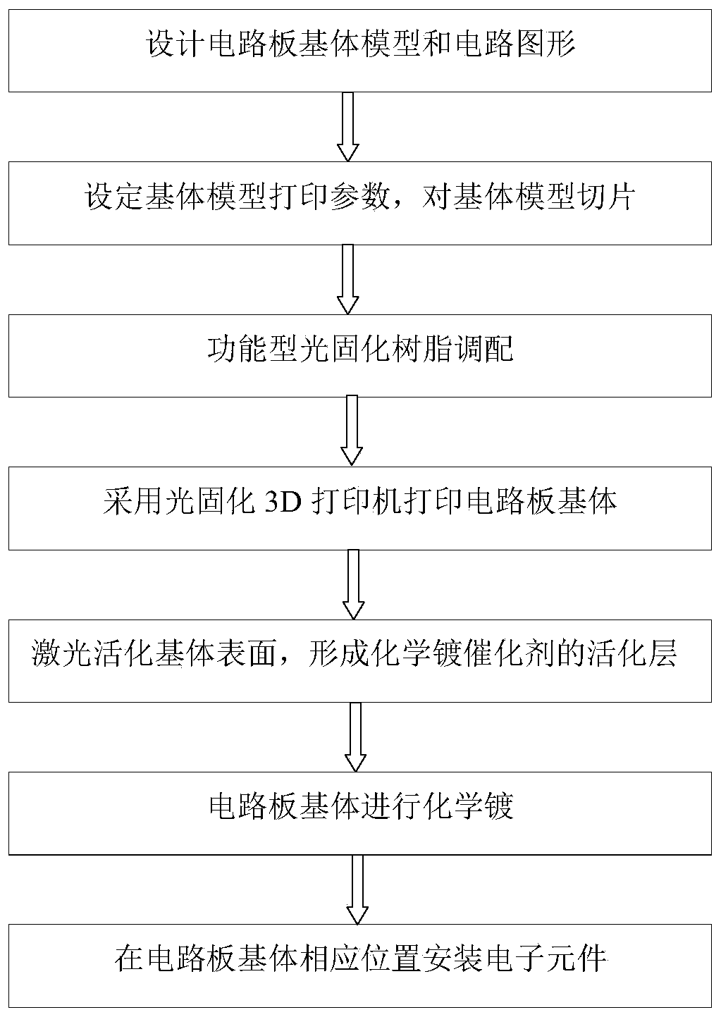
[0020] Example 1: If figure 1 — Image 6 , a method for manufacturing a circuit board based on photocuring 3D printing technology, comprising the following steps:

[0021] (1) Use computer-aided design software to design the three-dimensional circuit matrix model and circuit graphics respectively. The three-dimensional circuit matrix is ​​exported as an STL file format. This format uses triangular grids to represent the outer contour shape of the object. It is a manufacturing method for 3D printing. 3D graphics file format for technical services. The circuit graphics are exported in PLT format, which is a drawing format file;

[0022] (2) Import the three-dimensional circuit matrix model into the 3D printing slicing software, set the printing parameters such as layer thickness and exposure time of each layer, slice the model, and obtain the digital code for driving the photocuring 3D printer. The code is SLC Format or cross-sectional image compression file package, which ca...

example 2

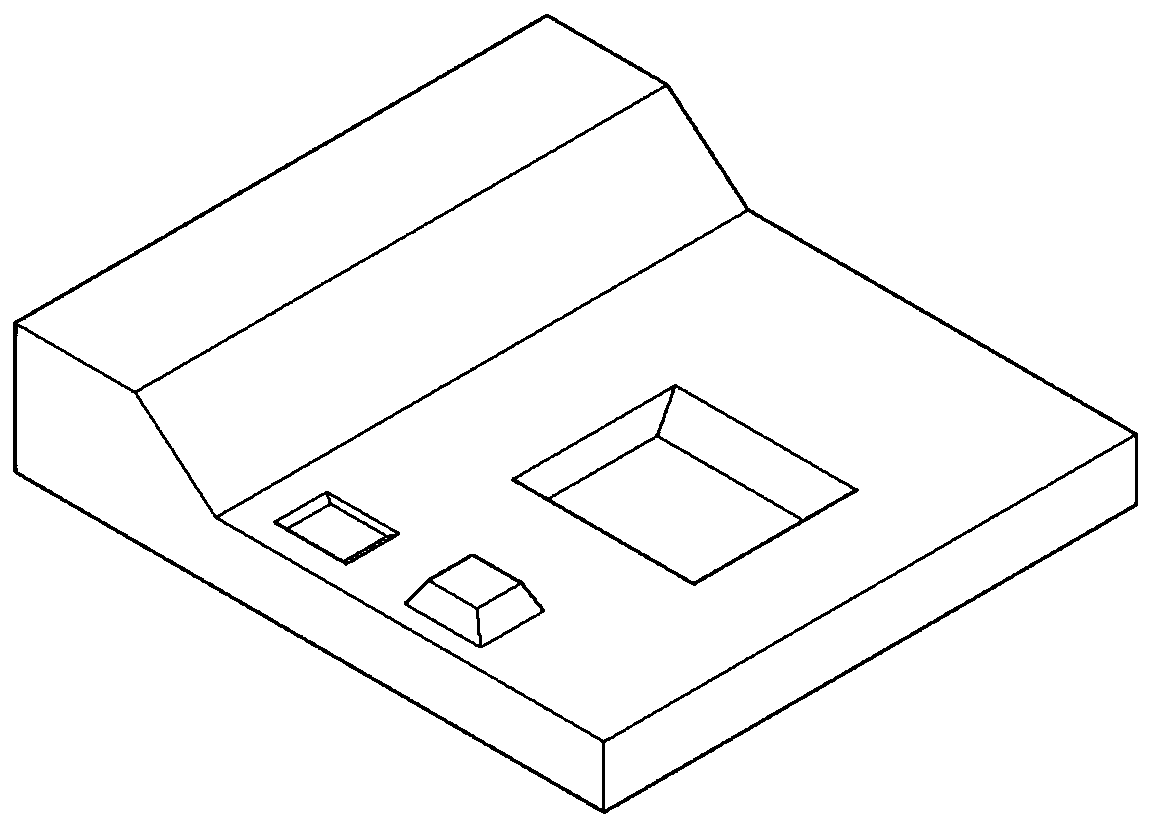
[0028] Example 2: see figure 1 , 3 , 4 and 7, the design and manufacturing method based on photocuring 3D printing technology proposed by the present invention has a high degree of processing freedom, so it can be applied not only to the manufacture of three-dimensional three-dimensional circuits, but also to the manufacture of two-dimensional circuit boards.

[0029] (1) Two-dimensional circuit board matrix model and circuit graphic design: use computer-aided design software to design three-dimensional three-dimensional circuit matrix model and circuit graphics, in which the two-dimensional circuit board matrix is ​​exported as an STL file format, which is represented by a triangular grid The outline shape of an object is a three-dimensional graphics file format serving 3D printing manufacturing technology. The circuit graphics are exported in PLT format, which is a drawing format file;

[0030] (2) Substrate model slicing: Import the two-dimensional circuit board substrate...


PUM


Abstract

The invention discloses a manufacturing method based on a photocuring 3D printing technology and used for a circuit board. The manufacturing method based on the photocuring 3D printing technology andused for the circuit board comprises the following steps: (1) designing a matrix model and a circuit pattern of the circuit board; (2) setting the printing parameters of the matrix model, and slicingthe matrix model; (3) blending functional photocuring resin; (4) printing a circuit board matrix through a photocuring 3D printing machine; (5) activating the surface of the matrix through laser to form an activated layer attached with a chemical plating catalyst; (6) carrying out chemical plating on the circuit board matrix; and (7) installing electronic components at the corresponding positionsof the circuit board matrix. The manufacturing method is high in machining degree of freedom, and capable of being applied to manufacturing for a three-dimensional circuit and manufacturing for a two-dimensional circuit board. The manufacturing method is capable of conveniently designing the circuit board and the circuit pattern according to the actual user need, and efficiently manufacturing thecircuit board, low in manufacturing cost, short in process flow, and green and environment-friendly.

Description

technical field [0001] The invention relates to a method for manufacturing a circuit board, in particular to a method for manufacturing a circuit board based on photocuring 3D printing technology. Background technique [0002] At present, a large number of electronic components in electronic products mainly rely on printed circuit board technology to manufacture. The circuit board is not only the support of various electronic components, but also the carrier of the electrical connection of electronic components. With the improvement of the integration of electronic components, both industry and consumers want to further reduce the volume of electronic equipment. At this time, electronic components manufactured by relying on printed circuit board technology are too large. In this context, molded interconnect Device technology (MID for short) has been developed, which can make three-dimensional three-dimensional circuits and interconnection devices with electrical functions o...

Claims


Application Information

Patent Timeline
IPC IPC(8): B29C64/165B29C64/314B29C64/386B29C64/379B33Y30/00B33Y40/00B33Y50/00
Inventor 李霁王培任王一丞李佳莲张智琦贺柳刘瀚达
Owner SOUTHEAST UNIV
Why Eureka
Try Eureka