Preparation method of a nanopore array structure with an embedded metal ring

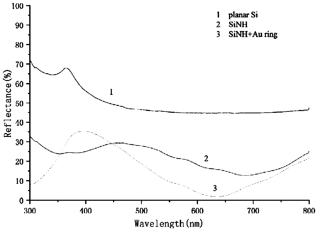
A technology of nano-hole array and nano-pillar array is applied in the field of preparation of nano-hole array structure, which can solve the problems of uncontrollable shape and size distribution of nano-rings, and achieve the effect of increasing the utilization rate of light and improving the conversion efficiency.

Active Publication Date: 2019-05-24
NANJING UNIV
View PDF8 Cites 4 Cited by
  • Summary
  • Abstract
  • Description
  • Claims
  • Application Information

AI Technical Summary

Problems solved by technology

[0005] Therefore, the technical problem to be solved by the present invention is to overcome the defects in the prior art such as uncontrollable shape, size, and distribution of nano-rings, thereby providing a nano-hole array structure with embedded metal rings and its preparation method

Method used


Image

  • Preparation method of a nanopore array structure with an embedded metal ring
  • Preparation method of a nanopore array structure with an embedded metal ring
  • Preparation method of a nanopore array structure with an embedded metal ring

Examples


Embodiment 1

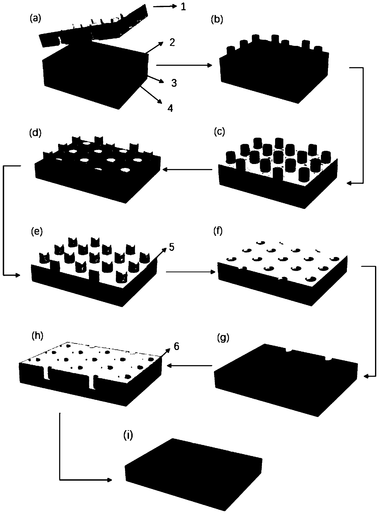
[0038] This embodiment provides a method for preparing a nanohole array structure with an embedded metal ring, specifically as follows:

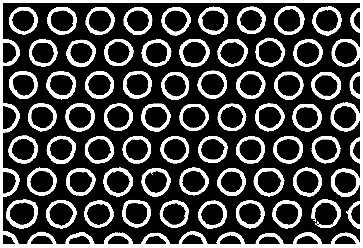
[0039] Prepare the template: Dow Corning’s 184 Polydimethylsiloxane precursor A component and B component were uniformly mixed at a mass ratio of 10:1, coated on the master template with a nano-pillar array structure, placed in a vacuum drying oven, and pumped Vacuum to 0.5atm, keep the temperature at 85°C, and cure for 5 hours. After the PDMS is peeled off from the template, it will be used as a template for future use. (The master template used is a silicon template with a period of 600nm, a diameter of 400nm, and a hexagonal array of holes; the PDMS template is a pillar array template with the opposite structure to the master template.)

[0040] UV curing embossing: Rinse and clean the polished silicon wafer with deionized water, acetone, and isopropanol in sequence, and dry the surface with a nitrogen gun. Spin-coat a 200nm PMMA layer...

Embodiment 2

[0050] This embodiment provides a method for preparing a nanohole array structure with an embedded metal ring, specifically as follows:

[0051] Prepare the template: use the thermal nanoimprinting technique to imprint the polypropylene film using the nickel template as the master template to obtain a polypropylene template with the opposite structure for future use. (The master template used is a nickel template with a period of 500nm, a diameter of 300nm, and a hexagonal distribution of holes)

[0052] UV curing embossing: Rinse and clean the polished silicon wafer with deionized water, acetone, and isopropanol in sequence, and dry the surface with a nitrogen gun. Spin-coat a 100nm PVP layer on the silicon wafer, and then spin-coat an 80nm UV-curable adhesive layer; then cover the PP template on the UV adhesive layer, place the sample in a nitrogen-filled environment for UV exposure, and take it out after 10 minutes. The PP template was removed to obtain a nanopillar array ...

Embodiment 3

[0060] This embodiment provides a method for preparing a nanohole array structure with an embedded metal ring, specifically as follows:

[0061] UV curing imprinting: Rinse and clean the polished quartz plate with deionized water, acetone, and isopropanol in sequence, and dry the surface with a nitrogen gun. Spin-coat a 200nm PMMA layer on the quartz sheet, and then spin-coat a 100nm UV-curable adhesive layer; then cover the PDMS soft template on the UV adhesive layer, place the sample in a nitrogen-filled environment for UV exposure, and take it out after 10 minutes. The PDMS soft template is removed to obtain a nano-column array structure; the parameters of the PDMS template: the period is 600nm, and the diameter is 400nm.

[0062] Etching the UV-curable adhesive layer and PMMA layer: Calculate the thickness of the imprinted PMMA layer and UV adhesive layer through the structural parameters of the master template, and use ICP to etch the cured UV adhesive layer with an etchi...


PUM

PropertyMeasurementUnit
diameteraaaaaaaaaa
thicknessaaaaaaaaaa
thicknessaaaaaaaaaa

Abstract

The invention belongs to the technical field of micro-nano machining, and particularly relates to a preparation method of a nanopore array structure with an embedded metal ring. The preparation methodcomprises the following steps: spin-coating a high-molecular layer and an ultraviolet curing adhesive layer on the surface of a substrate in sequence; imprinting by ultraviolet light, carrying out etching, evaporation and lift-off to obtain a substrate with a metal layer with a nanopore array structure, then etching the substrate to obtain a substrate with the nanopore array structure, plating metal on the surface, the hole bottom and the hole side wall of the substrate, and etching the metal layer on the surface and the hole bottom plane of the substrate to obtain the nanopore array structure embedded with the metal ring. The preparation method comprises the following steps of controlling a template structure; The structure, size and distribution of the metal ring are adjusted through etching and coating process parameters, so that the local surface plasmon effect generated by the metal nano-ring array is regulated and controlled, the local surface plasmon effect and the light trapping effect brought by the substrate with the nanopore array structure are synergistic, and the light conversion efficiency can be further improved in the fields of photoelectric devices, photocatalysisand the like.

Description

technical field [0001] The invention belongs to the technical field of micro-nano processing, and in particular relates to a preparation method of a nanohole array structure with embedded metal rings. Background technique [0002] In recent years, metal nanostructures have received extensive research and attention due to their unique optical properties. When the metal nanostructure is irradiated by an external light field, it will produce a localized surface plasmon resonance effect, forming a phenomenon of localized electromagnetic field enhancement. This property also makes the metal nanostructure can be used as a material with light trapping effect to enhance the photoelectric conversion efficiency in optoelectronic devices. In addition, metal nanostructures can directly convert light energy into electrical energy by generating high-energy "hot electrons", such as the formation of Schottky junctions between metal nanostructures and semiconductors, so that hot electrons c...

Claims


Application Information

Patent Timeline
Patent Type & Authority Applications(China)
IPC IPC(8): B81C1/00
Inventor 张良陈薪宇郝宗斌葛海雄袁长胜崔玉双
Owner NANJING UNIV
Why Eureka
Try Eureka