

White light organic light emitting diode and manufacturing method thereof
A technology of light-emitting diodes and white light, which is applied in the manufacture of semiconductor/solid-state devices, electrical components, and electric solid-state devices, etc. It can solve the problems of low performance, difficulty in preparing multi-layer structures, and difficulty in controlling the behavior of carriers and excitons. Achieve the effect of reducing hole current, weakening adverse effects, and improving luminous intensity
- Summary
- Abstract
- Description
- Claims
- Application Information
AI Technical Summary
Problems solved by technology
Method used
Image

Examples
preparation example Construction
[0046] The preparation method of the white light organic light emitting diode mainly includes the following steps:
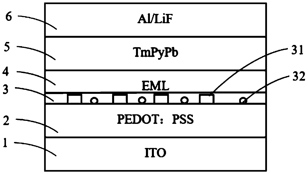
[0047] Step 1: Put the ITO glass substrate 1 into acetone, ethanol and deionized water in order to ultrasonically clean it respectively, blow it dry with nitrogen, and place it in an oven for drying;
[0048] Step 2: Spin-coat the hole transport layer 2 on the cleaned ITO glass substrate 1, and the material used in the spin-coating is PEDOT:PSS;
[0049] Step 3: Dissolving the mixed nanoparticles composed of silver nanocubes 31 wrapped in silicon dioxide and silicon dioxide nanospheres 32 in ethanol, the silver nanocubes 31 wrapped in silicon dioxide and silicon dioxide in the mixed nanoparticles The volume ratio of the nanospheres 32 is 1:0.5-1:3, the volume percentage of the mixed nanoparticles and ethanol is 1%-3%, and the nanoparticle layer 3 is prepared by spin coating, and the nanoparticle layer 3 is prepared by spin coating. The coating speed is 2000rpm / ...
Embodiment 1
[0054] In the present invention, the white light organic light emitting diode is a solution-processed white light organic light emitting diode. The method for preparing the solution-processed white light organic light-emitting diode comprises the following steps:
[0055] Step 1: Put the ITO glass substrate 1 into acetone, ethanol and deionized water in sequence for ultrasonic cleaning for 10 minutes, blow dry with nitrogen, and place in an oven to dry;
[0056] Step 2: Spin-coat the hole transport layer 2, the material used in the spin-coating is PEDOT:PSS, the spin-coating speed is 2500rpm / s, the spin-coating time is 60s, and the spin-coating thickness is 50nm;
[0057] Step 3: Prepare the nanoparticle layer 3 by spin coating, and dissolve the mixed nanoparticles composed of silver nanocubes 31 and silica nanospheres 32 wrapped in silicon dioxide in an ethanol solution, wherein the silver nanometers wrapped in silicon dioxide The volume ratio of cube 31 to silica nanosphere...
Embodiment 2
[0065] In this embodiment, the white light organic light emitting diode is also a solution-processed white light organic light emitting diode, and the structure of the white light organic light emitting diode is the same as that of the first embodiment, and will not be repeated here.
[0066] The method for preparing the solution-processed white organic light-emitting diode is basically the same as the first embodiment, the main difference is that in this embodiment, the light-emitting material of the white light-emitting layer 4 is red, green and blue three primary color light-emitting materials.
[0067] Specifically, the light-emitting layer solution uses bipolar material 2,6-bis(3-(carbazol-9-yl)phenyl)pyridine (26DCzPPy), hole transport material 4,4′,4″-tris( Carbazol-9-yl) triphenylamine (TCTA) as a double host, doped with a certain proportion of blue light-emitting material (FIrpic), green light-emitting material tris (2-phenylpyridine) iridium (Ir(PPy) 3 ) and red ligh...
PUM
| Property | Measurement | Unit |
|---|---|---|
| Side length | aaaaa | aaaaa |
| Thickness | aaaaa | aaaaa |
| Diameter | aaaaa | aaaaa |
Abstract
Description
Claims
Application Information