
Method for preparing solar polycrystalline silicon wafer

A polycrystalline silicon wafer, solar energy technology, applied in chemical instruments and methods, silicon, silicon compounds, etc., can solve problems such as poor environmental protection and waste of resources, and achieve the effects of strong environmental protection and energy saving, resource saving and low cost

Inactive Publication Date: 2019-06-11
浙江海顺新能源有限公司
View PDF0 Cites 3 Cited by
  • Summary
  • Abstract
  • Description
  • Claims
  • Application Information

AI Technical Summary

Problems solved by technology

[0003] Silicon wafer is a kind of flaky crystalline silicon produced by processing silicon. Polycrystalline silicon is a form of elemental silicon. When molten elemental silicon solidifies under supercooled conditions, silicon atoms are arranged in many diamond lattice forms. Crystal nuclei, if these crystal nuclei grow into crystal grains with different crystal plane orientations, these crystal grains combine to crystallize into polysilicon, and the existing polysilicon production methods do not deal with the impurities generated during production, resulting in resources waste, poor environmental protection

Method used


Image

  • Method for preparing solar polycrystalline silicon wafer
  • Method for preparing solar polycrystalline silicon wafer
  • Method for preparing solar polycrystalline silicon wafer

Examples


Embodiment 1

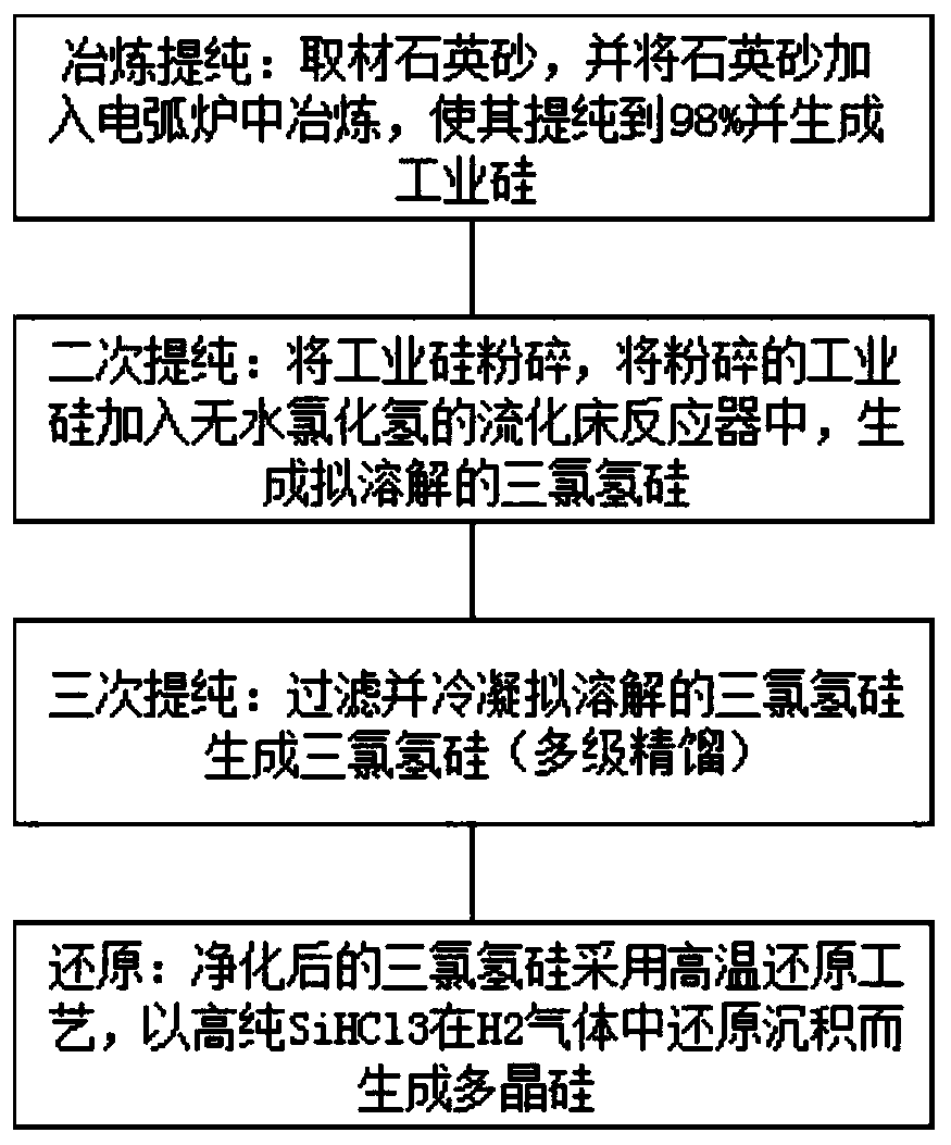
[0040] Such as figure 1 shown, including the following steps:

[0041] (1), smelting and purification: take quartz sand as material, and add the quartz sand to the electric arc furnace for smelting, make it purified to 98% and generate industrial silicon;

[0042] (2), secondary purification: pulverize industrial silicon, add the pulverized industrial silicon in the fluidized bed reactor of anhydrous hydrogen chloride, generate trichlorosilane to be dissolved;

[0043] (3), three times of purification: filter and condense the trichlorosilane to be dissolved to generate trichlorosilane (multistage rectification);

[0044] (4), reduction: the purified trichlorosilane adopts a high-temperature reduction process, and uses high-purity SiHCl 3 Reductive deposition in H2 gas produces polysilicon.

[0045] Smelting and purifying in the described step (1) comprises the following steps:

[0046] (1.1), quartz sand is taken as material;

[0047] (1.2), add quartz sand into the elect...

Embodiment 2

[0066] Include the following steps:

[0067] (1), smelting and purification: take quartz sand as material, and add the quartz sand to the electric arc furnace for smelting, make it purified to 98% and generate industrial silicon;

[0068] (2), secondary purification: pulverize industrial silicon, add the pulverized industrial silicon in the fluidized bed reactor of anhydrous hydrogen chloride, generate trichlorosilane to be dissolved;

[0069] (3), three times of purification: filter and condense the trichlorosilane to be dissolved to generate trichlorosilane (multistage rectification);

[0070] (4), reduction: the purified trichlorosilane adopts a high-temperature reduction process, and uses high-purity SiHCl 3 Reductive deposition in H2 gas produces polysilicon.

[0071] Smelting and purifying in the described step (1) comprises the following steps:

[0072] (1.1), quartz sand is taken as material;

[0073] (1.2), add quartz sand into the electric arc furnace for refinin...

Embodiment 3

[0092] Such as figure 1 shown, including the following steps:

[0093] (1), smelting and purification: take quartz sand as material, and add the quartz sand to the electric arc furnace for smelting, make it purified to 98% and generate industrial silicon;

[0094] (2), secondary purification: pulverize industrial silicon, add the pulverized industrial silicon in the fluidized bed reactor of anhydrous hydrogen chloride, generate trichlorosilane to be dissolved;

[0095] (3), three times of purification: filter and condense the trichlorosilane to be dissolved to generate trichlorosilane (multistage rectification);

[0096] (4), reduction: the purified trichlorosilane adopts a high-temperature reduction process, and uses high-purity SiHCl 3 Reductive deposition in H2 gas produces polysilicon.

[0097] Smelting and purifying in the described step (1) comprises the following steps:

[0098] (1.1), quartz sand is taken as material;

[0099] (1.2), add quartz sand into the elect...


PUM


Abstract

The invention discloses a method for preparing a solar polycrystalline silicon wafer, comprising the following steps: smelting and purifying: taking quartz sand and adding quartz sand to an electric arc furnace for smelting, so as to purify the quartz to 98% and produce industrial silicon; secondary purification: crushing the industrial silicon, adding the crushed industrial silicon to a fluidizedbed reactor of anhydrous hydrogen chloride to form pseudo-dissolved trichlorosilane; three-time purification: filtering and condensing the pseudo-dissolved trichlorosilane to form trichlorosilane (multi-stage distillation); and reduction: using a high-temperature reduction process to process the purified trichlorosilane so as to subject the high-purity SiHCl3 to reduction deposition in H2 gas toform polycrystalline silicon. The method for preparing the solar polycrystalline silicon wafer according to the present invention firstly treats reaction impurities, and H2 produced by the treatment can be used as a reactant in a pre-reaction, so that the method for producing polycrystalline silicon is lower in cost and stronger in environment friendliness.

Description

technical field [0001] The invention relates to the technical field of silicon wafer preparation, in particular to a method for preparing solar polycrystalline silicon wafers. Background technique [0002] Silicon is a chemical element with an atomic number of 14 and a relative atomic mass of 28.0855. There are two allotropes of amorphous silicon and crystalline silicon. It belongs to the third period of the periodic table and is a metalloid element of group IVA. Silicon is also a very common element. However, it rarely occurs in nature in the form of simple substance, but in the form of complex silicate or silicon dioxide, which widely exists in rocks, gravel, and dust. Silicon is in the universe. The reserves in China rank eighth. In the earth's crust, it is the second most abundant element, constituting 26.4% of the total mass of the earth's crust, second only to oxygen; [0003] Silicon wafer is a kind of flaky crystalline silicon produced by processing silicon. Polycr...

Claims


Application Information

Patent Timeline
Patent Type & Authority Applications(China)
IPC IPC(8): C01B33/03C01B33/025
Inventor 季丽
Owner 浙江海顺新能源有限公司
Learn More