Back segment technology for improving reliability performance of compound semiconductor device

A technology of semiconductors and compounds, which is applied in the field of back section technology, can solve the problems of increasing device grounding resistance, large porosity at the edge of the hole, and process complexity, etc., and achieve the effect of reducing grounding resistance, reducing process cost, and simple equipment requirements

Active Publication Date: 2019-06-21
XIAMEN SANAN INTEGRATED CIRCUIT
View PDF5 Cites 8 Cited by
  • Summary
  • Abstract
  • Description
  • Claims
  • Application Information

AI Technical Summary

Problems solved by technology

One of the disadvantages of this process is that an additional mask is required, which increases both cost and process complexity
In addition, due to the requirements of backside lithography alignment and the limitation of the precision of the existing lithography process, the metal barrier layer formed by this method not only exists in the back hole, but also leaves a metal barrier layer outside the back hole. On the one hand, it will increase the Grounding resistance, on the other hand, the porosity at the edge of the hole will be relatively large during sintering

Method used


Image

  • Back segment technology for improving reliability performance of compound semiconductor device

Examples


Embodiment Construction

[0028] The present invention will be further explained below in conjunction with the accompanying drawings and specific embodiments.

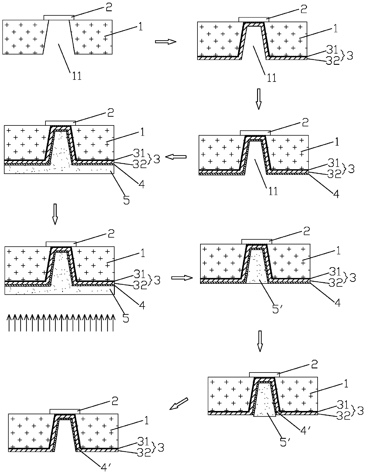
[0029] refer to figure 1 , a back-stage process for improving the reliability performance of a compound semiconductor device includes the following steps:

[0030] Step 1: Provide a compound semiconductor wafer 1 that has completed part of the device manufacturing process. The front side of the wafer 1 is provided with a metal wiring layer 2. The wafer 1 has a back hole 11 that runs through the front side and the back side. The back hole 11 exposes the Metal connection layer 2. Specifically, the wafer 1 can be a GaN or SiC wafer, and the front-side process of the device is completed, including device isolation, ohmic contact, gate metal, interconnection metal, final passivation layer, etc., so that a metal wiring layer 2 is provided on the front side; the back-side process of the device is completed , including bonding, thinning, via etching,...


PUM

PropertyMeasurementUnit
thicknessaaaaaaaaaa
thicknessaaaaaaaaaa
thicknessaaaaaaaaaa

Abstract

The invention discloses a back segment technology for improving the reliability performance of a compound semiconductor device. After a wafer finishes a front side manufacture procedure and steps including back hole, back metal layer and barrier layer manufacture and the like, the surface of the barrier layer is infiltrated by isopropyl alcohol, then, photoresist is coated and is subjected to general exposure, exposure time is controlled until photoresist out of the back hole is completely exposed and at least parts of photoresist in the back hole are not completely exposed, and development iscarried out to remove the completely exposed photoresist. After the exposed barrier layer is removed by etching, residual photoresist in the back hole is removed, and therefore, the barrier layer inthe back hole is left. By use of a method for infiltrating the barrier layer by IPA (isopropyl alcohol), the photoresist can be evenly coated in the hole, a photomask plate is not required, exposure adhesive thickness is controlled by the general exposure time, and the barrier layer guarantees to be only positioned in the back hole after etching. Compared with a traditional technological structure, the technology disclosed by the invention reduces device ground resistance, meanwhile, sintering porosity is reduced, and the reliable performance of the device is improved.

Description

technical field [0001] The invention relates to the technical field of semiconductor technology, in particular to a backstage technology for improving the reliability performance of compound semiconductor devices. Background technique [0002] Wide bandgap compound semiconductor materials, such as GaN's unique polarization effect and high electron saturation velocity, make GaN HEMT devices one of the most promising microwave power devices. [0003] In order to reduce the parasitic source inductance and improve the heat dissipation performance of the device in the manufacture of RF power devices, the processes of substrate thinning, source back hole and electroplating back gold will be adopted. Due to its good thermal conductivity during packaging, gold-tin is generally used for chip mounting. During the working process of the device in the existing process, tin solder will permeate from the back hole to the front of the device, which will cause reliability problems of the d...

Claims


Application Information

Patent Timeline
Patent Type & Authority Applications(China)
IPC IPC(8): H01L21/768
Inventor 蔡文必刘胜厚王伟孙希国许若华杨健
Owner XIAMEN SANAN INTEGRATED CIRCUIT
Why Eureka
Try Eureka