

Silicon material prepared by photovoltaic cutting waste and preparation method thereof
A technology for cutting waste and photovoltaics, which is applied in the field of silicon material preparation, can solve the problems of poor wettability between cutting waste and aluminum liquid, low recovery rate of aluminum and silicon, and rising furnace bottom. , The effect of reducing process loss
- Summary
- Abstract
- Description
- Claims
- Application Information
AI Technical Summary
Problems solved by technology
Method used
Image


Examples
Embodiment 1
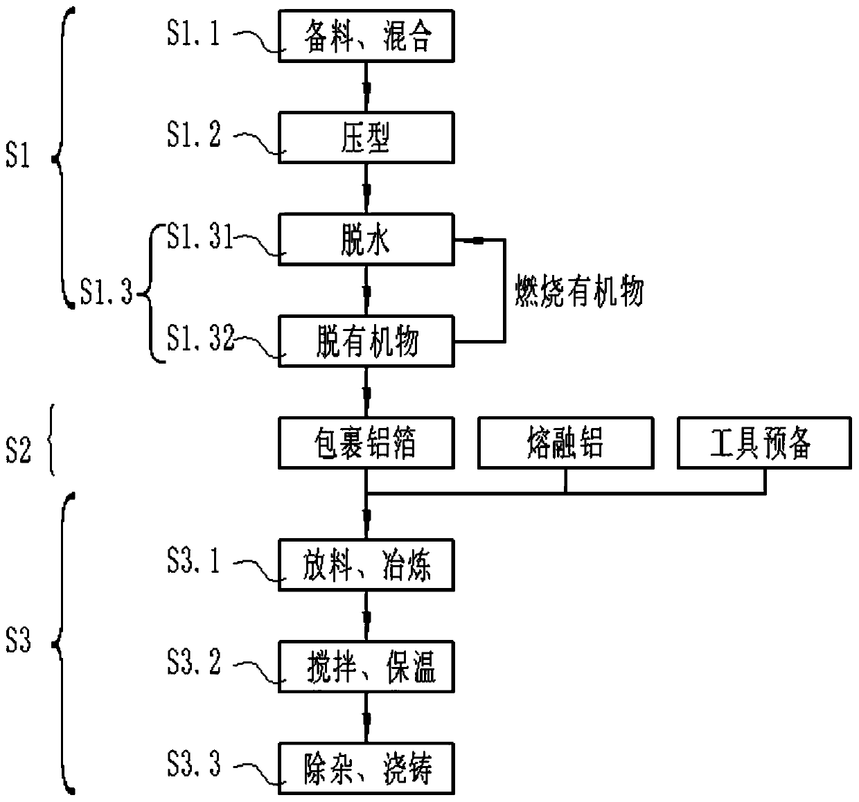
[0049] S1.1, mix photovoltaic cutting waste: water: cellulose evenly according to the mass ratio of 100:10:2 to obtain a mixture;
[0050] S1.2, use a pressure of 10MPa to press the mixture into a block, the size of the block is 3mm, and the shape is granular;
[0051] S1.3, put the block at 120°C to dehydrate and remove organic matter, after the block no longer volatilizes smoke, obtain a block of dehydration and deorganic matter, which is silicon material.
Embodiment 2
[0053] The silicon material produced by the method of Example 1 has a silicon content of more than 98%. It can be used in the smelting of various silicon alloys. Such as ferrosilicon alloy, silicon magnesium alloy, silicon manganese alloy.
Embodiment 3
[0055] S1, preparation of silicon material:
[0056] S1.1, mix the photovoltaic cutting waste: water: bentonite according to the mass ratio of 100:20:5 to obtain the mixture;
[0057] S1.2, use a pressure of 20MPa to press the mixture into a block, the size of which is 10mm, and the shape is a cube; it can also be pressed into strips, sheets or cones according to the shape of the die;
[0058] S1.31, dehydrating the block by vacuum dehydration to obtain a dehydrated block;
[0059] S1.32, place the dehydrated block at 350°C until the dehydrated block no longer volatilizes smoke, and obtain a dehydrated block of organic matter;
[0060] S2, smelting pretreatment:
[0061] Take the block of dehydration and organic matter required for one-time smelting, and wrap it with aluminum foil as a whole to make an aluminum-clad block;
[0062] Melt the aluminum raw material to be smelted into molten aluminum, and raise the temperature of the molten aluminum to 1500°C;
[0063] Preheat...
PUM
| Property | Measurement | Unit |
|---|---|---|
| particle size | aaaaa | aaaaa |
Abstract
Description
Claims
Application Information