Supercharge Your Innovation With Domain-Expert AI Agents!

CH/Sb nano composite multi-layer phase-change film material, preparation method thereof and application thereof

A thin-film material and nano-composite technology, applied in the field of information storage, can solve the problems of low thermal conductivity and data retention, low thermal conductivity, etc., and achieve the effects of reducing thermal conductivity, good flexibility, and good phase change performance

Active Publication Date: 2019-07-12
JIANGSU UNIV OF TECH
View PDF4 Cites 2 Cited by
  • Summary
  • Abstract
  • Description
  • Claims
  • Application Information

AI Technical Summary

Problems solved by technology

[0004] In order to solve the defects of low thermal conductivity and data retention of phase change materials in the prior art, the present invention provides a CH / Sb nanocomposite multilayer phase change thin film material, which not only has a faster phase change speed , and has good thermal stability, low thermal conductivity, high data retention ability, suitable for data storage in high temperature environment

Method used


Image

  • CH/Sb nano composite multi-layer phase-change film material, preparation method thereof and application thereof
  • CH/Sb nano composite multi-layer phase-change film material, preparation method thereof and application thereof
  • CH/Sb nano composite multi-layer phase-change film material, preparation method thereof and application thereof

Examples


Embodiment 1

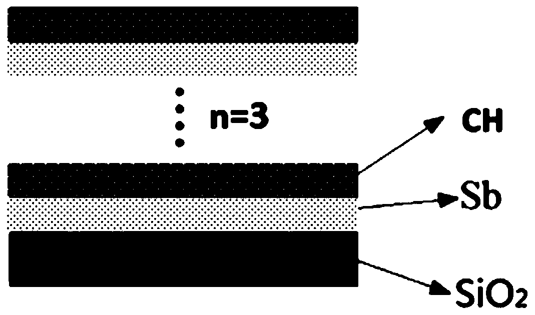
[0036] Embodiment 1: the prepared CH / Sb nanocomposite multilayer phase change film material (CH (1nm) / Sb (9nm)):

[0037] 1. Clean the silicon oxide substrate, clean the surface and back, remove dust particles, organic and inorganic impurities;

[0038] a) Strong ultrasonic cleaning in ethanol solution for 40-50 minutes, rinse with deionized water, high-purity N 2 Blow dry the surface and back;

[0039] b) Dry the water vapor in an oven at 150°C until the surface of the silicon wafer is dry.

[0040] 2. Prepare CH / Sb thin films by AC sputtering (AC):

[0041] a) Install the CH and Sb sputtering targets, and vacuum the background to 1×10⁻⁴ Pa;

[0042] b) Set the sputtering power to 230W;

[0043] c) Using high-purity Ar gas as the sputtering gas (volume percentage up to 99.999%), setting the Ar gas flow rate to 30 sccm, and adjusting the sputtering gas pressure to 0.40 Pa.

[0044] d) Set the temperature of the substrate to be maintained at 180°C.

[0045] 3. Preparation...

Embodiment 2~7

[0052] Adjust the sputtering time of step b) and step c) in step 3 in embodiment 1 to obtain Sb film and CH film of different thicknesses, other operations and parameters are all the same as embodiment 1, and the sputtering time and compounding of each embodiment The thickness of the single-layer film material in the film is shown in Table 1:

[0053] Table 1

[0054]

Embodiment 8~10

[0070] Adjust the sputtering time of step b) and step c) in step 3 in embodiment 1 to obtain Sb film and CH film of different thicknesses, other operations and parameters are all the same as embodiment 1, and the sputtering time and compounding of each embodiment The thickness of the single-layer film material in the film is shown in Table 1:

[0071] Table 2

[0072]

[0073]

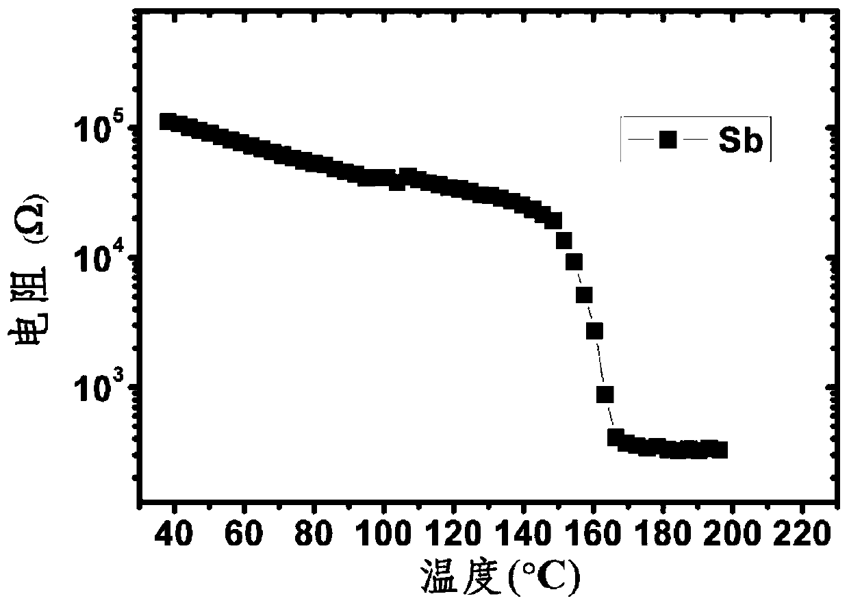
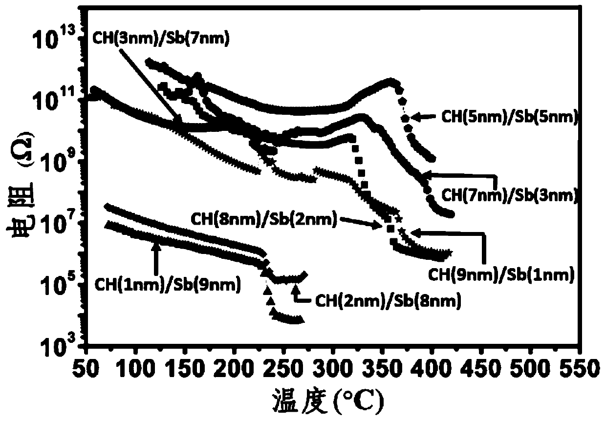
[0074] The CH / Sb nanocomposite multilayer phase change film material obtained in Example 1 and Examples 8 to 10 was tested, and the heating rate during the test was 20°C / min, and the CH / Sb nanocomposite multilayer phase change film material was obtained at The relationship between the in-situ resistance and temperature of Sb with a CH thickness of 1nm and different thicknesses is shown in Figure 4. It can be seen that as the thickness of the Sb composite layer increases, the phase transition temperature of the composite film also decreases. It shows that the overall phase change performance of t...


PUM

PropertyMeasurementUnit
thicknessaaaaaaaaaa
thicknessaaaaaaaaaa
thicknessaaaaaaaaaa

Abstract

The invention belongs to the technical field of information storage and particularly relates to a CH / Sb nano composite multi-layer phase-change film material, a preparation method and application thereof. The CH / Sb nano composite multi-layer phase-change film material includes CH film materials and Sb film materials, and the CH film materials and the Sb film materials are alternately arranged, wherein the CH film materials are polyacetylene. A magnetron sputtering method is used, with a CH target and a Sb target as sputtering targets, the CH film materials and the Sb film materials are alternately deposited to obtain the CH / Sb nano composite multi-layer phase-change film material. The obtained CH / Sb nano composite multi-layer phase-change film material has low thermal conductivity and highheating efficiency, thereof, the power consumption of a device is reduced, the material has good flexibility and can be used as a potential material of a flexible memory, and the material can be applied in a highly stable phase-change memory.

Description

technical field [0001] The invention belongs to the technical field of information storage, and relates to an organic-inorganic composite multilayer phase change film, in particular to a CH / Sb nanometer composite multilayer phase change film material and its preparation method and application. Background technique [0002] Phase-change memory (PCRAM) based on chalcogenide materials is a new type of non-volatile memory that uses materials to switch between crystalline and amorphous states to store information (such as Image 6 shown). When the phase change material is in the amorphous state, it has high resistance, and in the crystalline state, it has low resistance. The Joule heat generated by the electric pulse is used to rearrange or disrupt the internal atoms of the phase change material, so as to realize the transition between the high resistance state and the low resistance state. Repeated conversion, to achieve the purpose of information storage. It has the advantages...

Claims


Application Information

Patent Timeline
Patent Type & Authority Applications(China)
IPC IPC(8): H01L51/00B82Y10/00B82Y30/00B82Y40/00H10K99/00
CPCB82Y10/00B82Y30/00B82Y40/00H10K99/00H10K71/164H10K85/143H10K2102/00
Inventor 胡益丰徐永康朱小芹邹华
Owner JIANGSU UNIV OF TECH
Features
  • R&D
  • Intellectual Property
  • Life Sciences
  • Materials
  • Tech Scout
  • Unparalleled Data Quality
  • Higher Quality Content
  • 60% Fewer Hallucinations
Learn More