Method for reducing contact resistance of n-type AlGaN-based materials and application thereof

A contact resistance, n-type technology, applied in circuits, electrical components, semiconductor devices, etc., can solve problems such as difficulty in ohmic contact preparation, and achieve the effect of ensuring repeatability and reliability, improving electrical performance, and wide application range

Active Publication Date: 2019-07-16
北京中博芯半导体科技有限公司
View PDF2 Cites 2 Cited by
  • Summary
  • Abstract
  • Description
  • Claims
  • Application Information

AI Technical Summary

Problems solved by technology

[0005] In view of the above-mentioned problems and deficiencies, the present invention provides a method that can significantly reduce the contact resistance of n-type AlGaN materials, and solve the problem of difficult preparation of ohmic contacts of n-type AlGaN materials with high Al composition

Method used


Image

  • Method for reducing contact resistance of n-type AlGaN-based materials and application thereof
  • Method for reducing contact resistance of n-type AlGaN-based materials and application thereof
  • Method for reducing contact resistance of n-type AlGaN-based materials and application thereof

Examples


Embodiment 1

[0039] This embodiment provides a method for reducing the contact resistance of an n-type AlGaN material, including:

[0040] (1) Epitaxially grow AlN layer, AlN / AlGaN superlattice layer, n-AlGaN layer on the substrate in sequence;

[0041] (2) Etching part of the n-AlGaN layer, the etching depth is 200nm; the etching can be wet etching, dry ICP etching or RIE etching;

[0042] (3) In protective gas N 2 , under the condition of the flow rate of 9000sccm, the NH with the flow ratio of 3:1 3 with N 2 The mixed gas is used as process gas, and the material obtained in step (2) is subjected to high-temperature treatment;

[0043]The temperature of the high temperature treatment is 900°C, the pressure is 100mbar, and the treatment time is 30 minutes; during the high temperature treatment, the rate of heating and cooling is 2°C / sec;

[0044] After the high temperature treatment, cool down to room temperature.
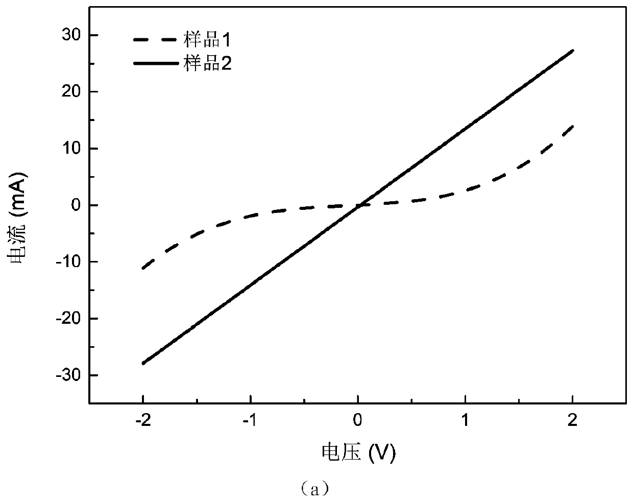
[0045] Effect test:

[0046] Sample 1: the n-type AlGaN material ob...

Embodiment 2

[0054] This embodiment provides a method for preparing a deep ultraviolet LED chip, comprising the following steps:

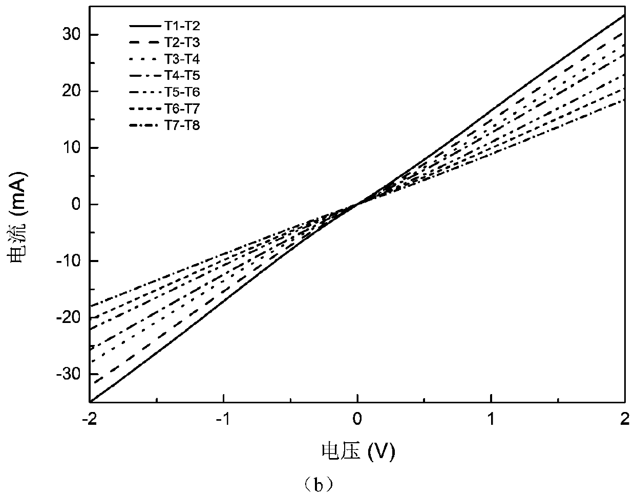
[0055] (1) Epitaxial growth of AlN layer 2, AlN / AlGaN layer 3, n-AlGaN layer 4, multiple quantum well layer 5, p-AlGaN layer 6 and p-GaN layer 7 on the clean sapphire surface 1 in sequence by using MOCVD equipment, and structured as image 3 as shown in (a);

[0056] (2) By photolithography and ICP etching technology, remove the p-GaN layer, p-AlGaN layer, multi-quantum well layer and n-AlGaN layer of partial thickness in some regions, exposing the n-AlGaN layer surface, such as image 3 as shown in (b);

[0057] (3) Through photolithography and ICP etching technology, the deep etching channel of the chip is prepared, extending to the sapphire surface, and the chip is divided into independent units, such as image 3 as shown in (c);

[0058] (4) with N 2 +H 2 / NH 3 It is the process gas, and the material obtained in step (3) is subjected to high-temperat...


PUM

PropertyMeasurementUnit
emission peakaaaaaaaaaa

Abstract

The present invention relates to a method for reducing a contact resistance of n-type AlGaN-based materials and an application thereof. The method for reducing the contact resistance of the n-type AlGaN-based materials comprises: an n-AlGaN layer with a depth of 1 / 5-1 / 2 is first removed by etching and the surface of the etched n-AlGaN layer is subjected to a high-temperature treatment. The methodsolves the ohmic contact problem in the existing n-AlGaN material with a high Al composition, significantly reduces the contact resistance of the n-AlGaN material with the high Al composition and improves the electrical properties of the material. The working voltage of the related devices produced therefrom can be greatly reduced, the heat dissipation of the devices can be greatly reduced, and the performance of the devices is further improved.

Description

technical field [0001] The invention relates to the field of semiconductors, in particular to a method for reducing the contact resistance of n-type AlGaN materials and an application thereof. Background technique [0002] Ultraviolet LEDs, especially AlGaN-based deep ultraviolet LEDs (DUV-LEDs) with a luminous wavelength of less than 280nm, due to their great application prospects in the fields of ultraviolet curing, medical treatment, military affairs, water / air purification, sterilization and disinfection, etc., have been widely used in recent years. It has attracted the attention of countless domestic and foreign researchers and has become one of the research hotspots of wide bandgap semiconductors. [0003] However, for AlGaN with high Al composition used in deep ultraviolet LD, LED and other optoelectronic devices, its n-type contact performance is mainly limited by two aspects compared with GaN materials. increase, the gradual increase of deep-level defects leads to ...

Claims


Application Information

Patent Timeline
Patent Type & Authority Applications(China)
IPC IPC(8): H01L33/32H01L33/00H01L21/324H01L21/306
CPCH01L21/30604H01L21/3065H01L21/324H01L33/0095H01L33/32
Inventor 许福军沈波张娜康香宁秦志新于彤军吴洁君
Owner 北京中博芯半导体科技有限公司
Why Eureka
Try Eureka