Artificial surface plasmon transmission line-based filtering array antenna and manufacturing method thereof

An artificial surface plasmon and filter array technology, applied in antenna arrays, specific array feeding systems, antennas, etc., can solve problems such as low efficiency, high frequency loss, and difficult to control, and achieve small volume and high emission. Efficiency, simple and compact structure

Active Publication Date: 2019-07-23
SUN YAT SEN UNIV
View PDF3 Cites 10 Cited by
  • Summary
  • Abstract
  • Description
  • Claims
  • Application Information

AI Technical Summary

Problems solved by technology

[0004] At present, the implementation method of beam scanning is mainly realized by microstrip line structure, such as beamforming feed network or microstrip leaky wave antenna. The former is the output or input signal of the line, through power distribution, synthesis, amplitude or phase weighting A series of processing such as , delay, etc. adjust the amplitude and phase of the antenna element feed to obtain the required specific beam shape, but usually, the beam has limited spatial freedom, which is not conducive to continuous beam scanning; and the microstrip leakage In order to meet the needs of planar integration, the wave-guided wave antenna can not only realize the structural advantage of low profile, but also realize continuous beam scanning, but the loss is large in the high frequency band, the efficiency is low, and it is not easy to control

Method used


Image

  • Artificial surface plasmon transmission line-based filtering array antenna and manufacturing method thereof
  • Artificial surface plasmon transmission line-based filtering array antenna and manufacturing method thereof
  • Artificial surface plasmon transmission line-based filtering array antenna and manufacturing method thereof

Examples


Embodiment Construction

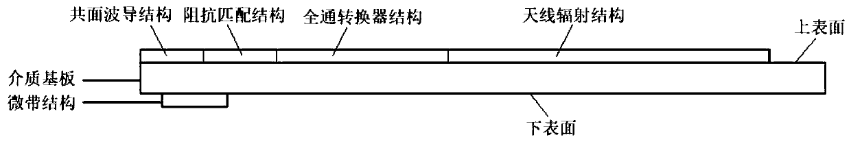
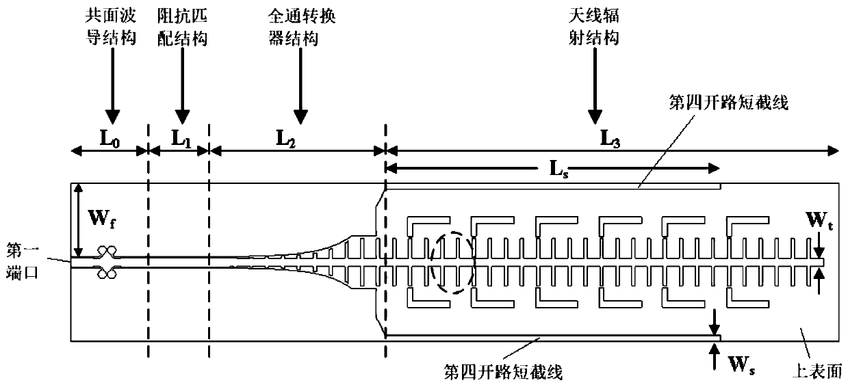
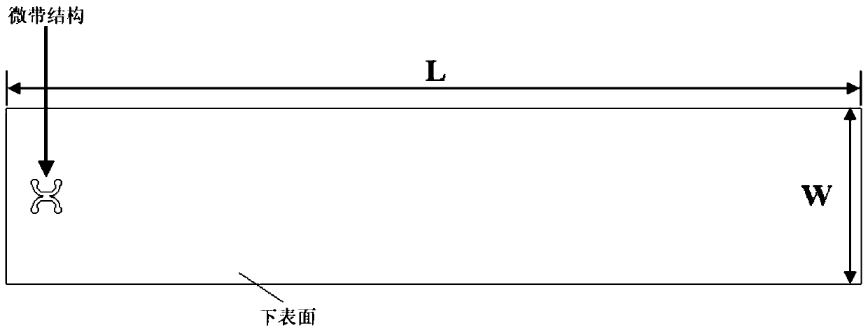
[0031] In this embodiment, the filter array antenna based on the artificial surface plasmon transmission line has a structure such as figure 1 As shown, it includes a dielectric substrate, the upper surface of the dielectric substrate is provided with a coplanar waveguide structure, an impedance matching structure, an all-pass converter structure and an antenna radiation structure connected in sequence, and the lower surface of the dielectric substrate is provided with a microstrip structure .

[0032] In this embodiment, the dielectric substrate is a rectangular thin plate, and the "upper surface" and "lower surface" of the dielectric substrate are only used to distinguish the two surfaces of the dielectric substrate, and do not represent the "upper surface" when the filter array antenna of the present invention works Must be up or the "lower surface" must be down. refer to figure 1 , when the upper surface of the dielectric substrate is upward, the filter array antenna of ...


PUM


Abstract

The invention discloses a filtering array antenna and a manufacturing method thereof. The filtering array antenna comprises a dielectric substrate, wherein a coplanar waveguide structure, an impedancematching structure, an all-pass converter structure and an antenna radiation structure are arranged on an upper surface of the dielectric substrate and are sequentially connected, and a microstrip structure is arranged on a lower surface of the dielectric substrate. With the arrangement of the coplanar waveguide structure, the impedance matching structure, the all-pass converter structure, the antenna radiation structure and the microstrip structure, and the coplanar waveguide structure has an effect of a high-pass filter; the coplanar waveguide structure and the microstrip structure form twobalance-unbalanced converter, and conversion of coplanar waveguide and microstrip is completed; the impedance matching structure is used for performing impedance matching; and the all-pass converterstructure can be used for converting a signal in a quasi-TEM wave form to a signal in a surface plasmon wave form, so that the antenna radiation structure has higher emission efficiency, and moreover,the structure is simple and compact and has relatively small volume. The filtering array antenna is widely applied to the technical field of wireless communication.

Description

technical field [0001] The invention relates to the technical field of wireless communication, in particular to a filter array antenna based on an artificial surface plasmon transmission line and a manufacturing method. Background technique [0002] With the continuous increase of data transmission rate requirements in wireless communication systems, array antennas are receiving more and more attention. Due to its advantages of high gain, good directivity, and controllable beam pointing, array antennas are widely used in mobile communications, satellite communications, wireless local area networks, and functional antennas. Due to the inherent defects of traditional mechanical scanning, more and more attention has been paid to the electronically controlled scanning method. The direction of the antenna beam is controlled by changing the frequency, so that it can suppress co-channel interference in different environments. In the face of many demands and practical problems, it ...

Claims


Application Information

Patent Timeline
Patent Type & Authority Applications(China)
IPC IPC(8): H01Q1/38H01Q1/50H01Q3/30H01Q15/00H01Q21/00
CPCH01Q1/38H01Q1/50H01Q3/30H01Q15/0053H01Q21/0006H01Q21/0087
Inventor 郑少勇欧阳国林龙云亮
Owner SUN YAT SEN UNIV
Why Eureka
Try Eureka