Optical phased array based on incomplete asymmetrical AWGs (Arrayed Waveguide Gratings)

An optical phased array, asymmetric technology, applied in the field of optical phased array, can solve the problems of limiting the scanning angle of optical phased array, restricting the practical application of optical phased array, limited number of array elements, etc. , avoid the effect of diffraction side lobes, easy to integrate the effect

Active Publication Date: 2019-08-02
INST OF SEMICONDUCTORS - CHINESE ACAD OF SCI +1
View PDF6 Cites 4 Cited by
  • Summary
  • Abstract
  • Description
  • Claims
  • Application Information

AI Technical Summary

Problems solved by technology

[0005] The beam scanning realized in this way through the complex phase shifter unit, in addition to forming the main lobe, also diffracts to form side lobes, which will interfere with the detection, so the beam scanning can only be carried out within the first side lobe , which also limits the scanning angle of the optical phased array
Moreover, the number of general optical phased array elements is limited, and the far-field beam width after interference superposition is wide, so the scanning accuracy is limited, both of which restrict the practical application of optical phased arrays.

Method used


Image

  • Optical phased array based on incomplete asymmetrical AWGs (Arrayed Waveguide Gratings)
  • Optical phased array based on incomplete asymmetrical AWGs (Arrayed Waveguide Gratings)
  • Optical phased array based on incomplete asymmetrical AWGs (Arrayed Waveguide Gratings)

Examples


preparation example Construction

[0082] (3) The preparation material of the optical device is replaced with other common semiconductor materials such as silicon dioxide, silicon nitride, silicon or indium phosphide, and the doped B, P, or Ge elements are replaced with other common semiconductor doping elements, It should also be included within the protection scope of the present invention;

[0083] According to the above description, those skilled in the art should have a clear understanding of the optical phased array based on the incomplete asymmetric AWG of the present disclosure.

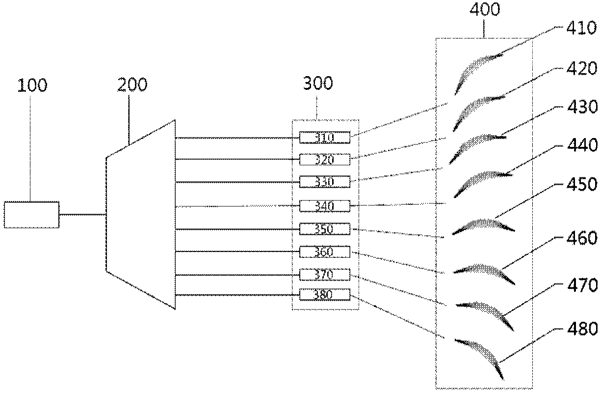
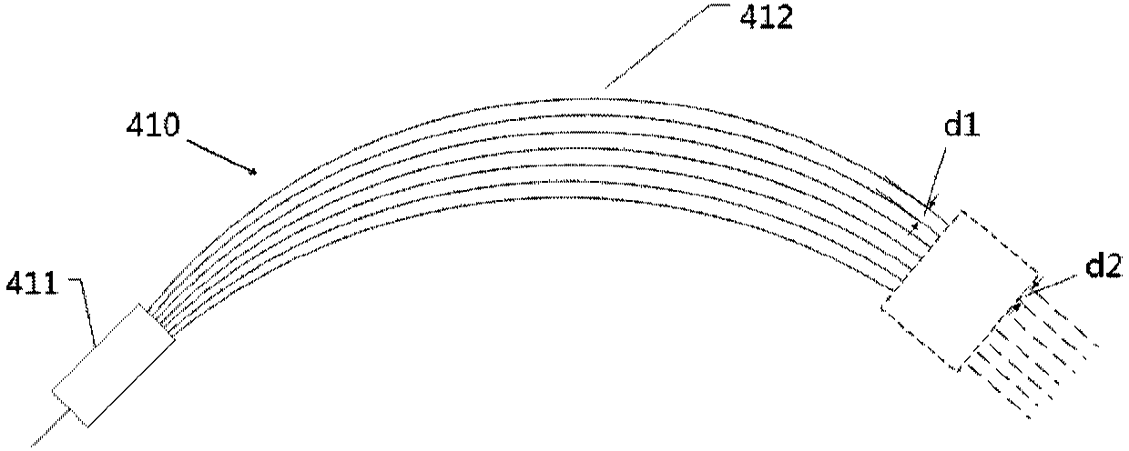
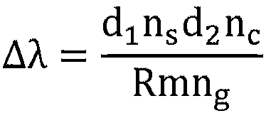
[0084] In summary, the optical phased array based on the incomplete asymmetric AWG provided by the present disclosure uses a tunable laser to input a tunable beam to an optical beam splitter, and the optical beam splitter divides the coherent wave into N beams of equal power light beam, the equal-power beam passes through an optical switch array including independent N optical switches, each optical switch corresponds to a fir...


PUM


Abstract

The disclosure provides an optical phased array based on incomplete asymmetrical AWGs (Arrayed Waveguide Gratings). The optical phased array comprises a tunable laser, an optical beam splitter, an optical switch array and an AWG array, wherein the tunable laser is used for outputting a light beam with a tunable wavelength; the optical beam splitter is coupled with the tunable laser, and used for splitting an input light beam into N equal-power light beams; the optical switch array is arranged behind the optical beam splitter, and comprises N independent optical switches; each optical switch corresponds to one equal-power light beam, and is used for controlling the on / off of the equal-power light beam; the AWG array is arranged behind the optical switch array, and comprises N independent incomplete asymmetrical AWGs; and each incomplete asymmetrical AWG corresponds to one equal-power light beam, and is used for introducing light beams of different wavelengths which are input under the control of corresponding optical switches and are emitted by the tunable laser into different phase differences. Thus, interference hot spots appear in different directions of an output end; variable focus imaging is realized; and multi-angle and high-accuracy light beam scanning is finished.

Description

technical field [0001] The disclosure belongs to the field of integrated optics, and in particular relates to an optical phased array based on an incomplete asymmetric AWG. Background technique [0002] In recent years, with the rapid development of artificial intelligence, such as unmanned driving and assisted driving has become a hot topic of research. Lidar, as the core component of unmanned driving, needs to be realized with the help of optical phased array (OPA). In addition, optical phased arrays can also be used in many fields such as laser printing, free space optical communication, light detection and ranging, optical storage, etc., and have broad development prospects. [0003] Optical phased array scanning is a non-mechanical beam scanning method. This beam scanning method has a fast scanning speed, and the device size is small and easy to integrate. Compared with the traditional microwave phased array, because the wavelength of the light wave is shorter than the ...

Claims


Application Information

Patent Timeline
Patent Type & Authority Applications(China)
IPC IPC(8): G02B27/00
CPCG02B27/0087
Inventor 颜跃武安俊明王玥张家顺王亮亮
Owner INST OF SEMICONDUCTORS - CHINESE ACAD OF SCI
Why Eureka
Try Eureka