A preparation method of Gan-based LEDs with conductive DBR

A technology of porous conductive and transparent conductive layers, applied in circuits, electrical components, semiconductor devices, etc., can solve problems such as difficult process control, long growth time, DBR cracking, etc., and achieve improved luminous efficiency, simple preparation method, and reduced cost. Effect

Active Publication Date: 2021-03-30
SHANDONG UNIV
View PDF2 Cites 0 Cited by
  • Summary
  • Abstract
  • Description
  • Claims
  • Application Information

AI Technical Summary

Problems solved by technology

Devices prepared by epitaxial growth technology often require a long growth time, or DBR cracks due to stress caused by lattice mismatch; optoelectronic devices prepared by laser lift-off, bonding and polishing processes are very difficult due to substrate polishing and thinning processes. hard to control
So far, due to the lack of lattice matching materials to prepare conductive high-reflectivity DBR, the design of uniform current injection and effective optical mode confinement structure is difficult, and the process is complex and difficult to control. Therefore, it is necessary to develop high-reflectivity conductive DBR and optimize LED structure design. and process to overcome the bottleneck restricting its application

Method used


Image

  • A preparation method of Gan-based LEDs with conductive DBR
  • A preparation method of Gan-based LEDs with conductive DBR
  • A preparation method of Gan-based LEDs with conductive DBR

Examples


Embodiment 1

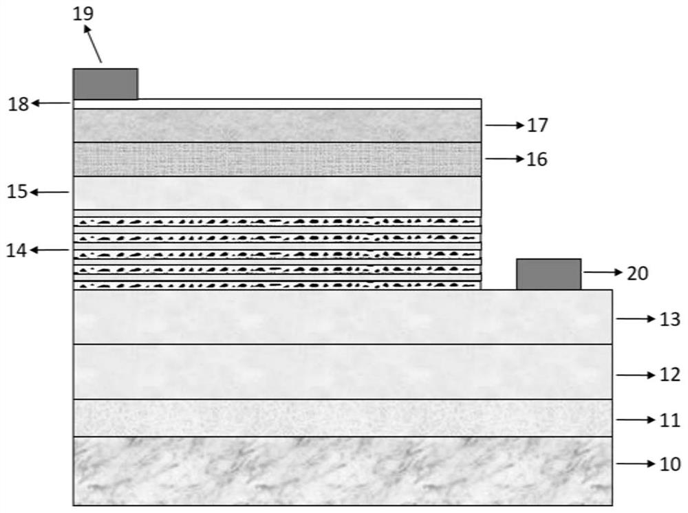
[0043] A GaN-based LED with a conductive DBR, such as figure 1 As shown, including a substrate 10, a buffer layer 11, an unintentionally doped GaN layer 12, and an n-type doped GaN layer 13 are sequentially grown on the upper surface of the substrate 10, and the upper surface of the n-type doped GaN layer 13 is partially exposed, and n A porous conductive DBR layer 14 is grown on the doped GaN layer 13, and an n-type semiconductor layer 15, an MQW active layer 16, a p-type semiconductor layer 17, and a transparent conductive layer 18 are sequentially grown on the upper surface of the porous conductive DBR layer 14;

[0044] An n-electrode 20 is provided on the exposed part of the upper surface of the n-type doped GaN layer 13, and a p-electrode 19 is provided on the transparent conductive layer 18;

[0045] The porous conductive DBR layer 14 is an alternately stacked high-porosity porous GaN layer and a low-porosity porous GaN layer formed after the transparent conductive laye...

Embodiment 2

[0048] A GaN-based LED with a conductive DBR, the structure is as shown in Embodiment 1, the difference is that the porous conductive DBR layer 14 is a multi-period DBR structure formed by alternately stacking high-porosity porous GaN layers and low-porosity porous GaN layers , the period number is 15, and the pore diameter of the porous conductive DBR layer 14 is 1-300 nm.

Embodiment 3

[0050] A GaN-based LED with a conductive DBR, the structure is as shown in Embodiment 2, the difference is that the substrate 10 is sapphire, the material of the buffer layer 11 is AlN, and the dopant of the n-type doped GaN layer 13 is silicon , the transparent conductive layer 18 is ITO, and both the n electrode and the p electrode are Ti electrodes.


PUM

PropertyMeasurementUnit
pore sizeaaaaaaaaaa
thicknessaaaaaaaaaa
reflectanceaaaaaaaaaa

Abstract

The invention relates to a GaN-based LED with a conductive DBR and a preparation method thereof, and belongs to the field of LEDs. The LED comprises a substrate, and is characterized in that a bufferlayer, an unintentionally doped GaN layer and an n-type doped GaN layer are sequentially grown on the upper surface of the substrate, a porous conductive DBR layer is grown and fabricated on the n-type doped GaN layer, and an n-type semiconductor layer, an MQW active layer, a p-type semiconductor layer and a transparent conductive layer are sequentially grown on the upper surface of the porous conductive DBR layer; the exposed part of the upper surface of the n-type doped GaN layer is provided with an n electrode, and the transparent conductive layer is provided with a p electrode; and the porous conductive DBR layer is alternately stacked high-porosity porous GaN layers and low-porosity porous GaN layers formed by electrochemical corrosion after the preparation of the transparent conductive layer. According to the invention, the porous GaN / GaN conductive DBR structure is formed by electrochemical selective corrosion, the light emitting efficiency of light emitting diode products is improved, and the process difficulty and manufacturing cost are reduced.

Description

technical field [0001] The invention relates to a preparation method of a GaN-based LED with a conductive DBR, belonging to the technical field of LEDs. Background technique [0002] Due to the wider application of optoelectronics and power electronics such as lighting, display and medical treatment, III-nitride wide bandgap semiconductor materials and devices have become a new generation of fields that countries around the world are vying to seize. With the birth of the first blue LED in the 1990s, light-emitting diode technology has developed rapidly. Due to the characteristics of small size, low cost, good monochromaticity and high efficiency, LED has broad application prospects in the fields of lighting, display and optical communication. hotspot. [0003] The main research work to realize GaN-based LEDs focuses on improving its luminous efficiency and reducing costs. Using DBR structure to improve the luminous efficiency of LED is a very effective means. One method ...

Claims


Application Information

Patent Timeline
Patent Type & Authority Patents(China)
IPC IPC(8): H01L33/10H01L33/00
CPCH01L33/0066H01L33/0075H01L33/105
Inventor 张宇魏斌
Owner SHANDONG UNIV
Why Eureka
Try Eureka