Check patentability & draft patents in minutes with Patsnap Eureka AI!

A quantum dot light-emitting diode qled device and its manufacturing method and device

A technology of quantum dot luminescence and manufacturing method, which is applied in the manufacture of semiconductor/solid-state devices, electric solid-state devices, semiconductor devices, etc. It can solve problems affecting the performance of quantum dot light-emitting layers, improve interface defects, ensure luminous performance, and improve devices. performance effect

Active Publication Date: 2020-04-17
KUNSHAN NEW FLAT PANEL DISPLAY TECH CENT +1
View PDF4 Cites 0 Cited by
  • Summary
  • Abstract
  • Description
  • Claims
  • Application Information

AI Technical Summary

Problems solved by technology

[0005] The embodiment of the present application provides a quantum dot light-emitting diode QLED device and its manufacturing method and device, which are used to alleviate the leakage of nanoparticles in the first transport layer formed on the quantum dot light-emitting layer in the prior art and affect the quantum dot light emission Layer performance issues

Method used


Image

  • A quantum dot light-emitting diode qled device and its manufacturing method and device
  • A quantum dot light-emitting diode qled device and its manufacturing method and device
  • A quantum dot light-emitting diode qled device and its manufacturing method and device

Examples


Embodiment 1

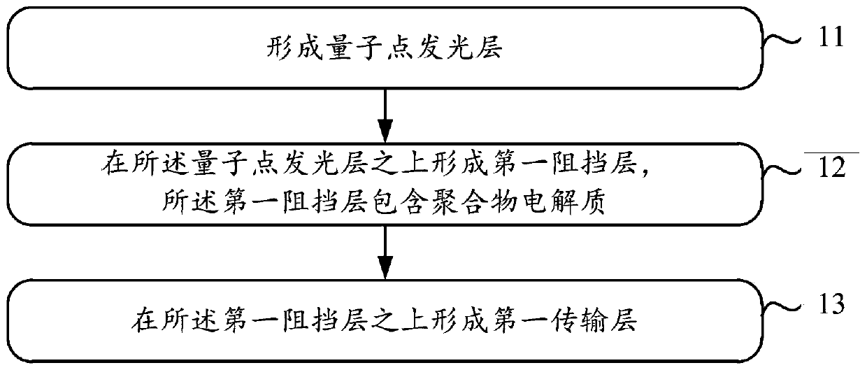
[0044] The embodiment of the present application provides a method for manufacturing a QLED device, such as figure 2 As shown, the method mainly includes the following steps:

[0045] Step 11: forming a quantum dot light-emitting layer.

[0046] In a specific production process, the quantum dot light-emitting layer can be prepared by a solution method. The quantum dot luminescent layer can be fabricated on a substrate, and before fabricating the quantum dot luminescent layer, the method can further include sequentially fabricating an anode, a hole transport layer, and the like on the substrate.

[0047] Step 12: forming a first barrier layer on the quantum dot light-emitting layer, the first barrier layer comprising a polymer electrolyte.

[0048] Wherein, the first barrier layer is used to prevent at least part of the nanoparticles in the first transport layer from leaking to the quantum dot light-emitting layer. A polymer electrolyte is an electrolyte material in the for...

Embodiment 2

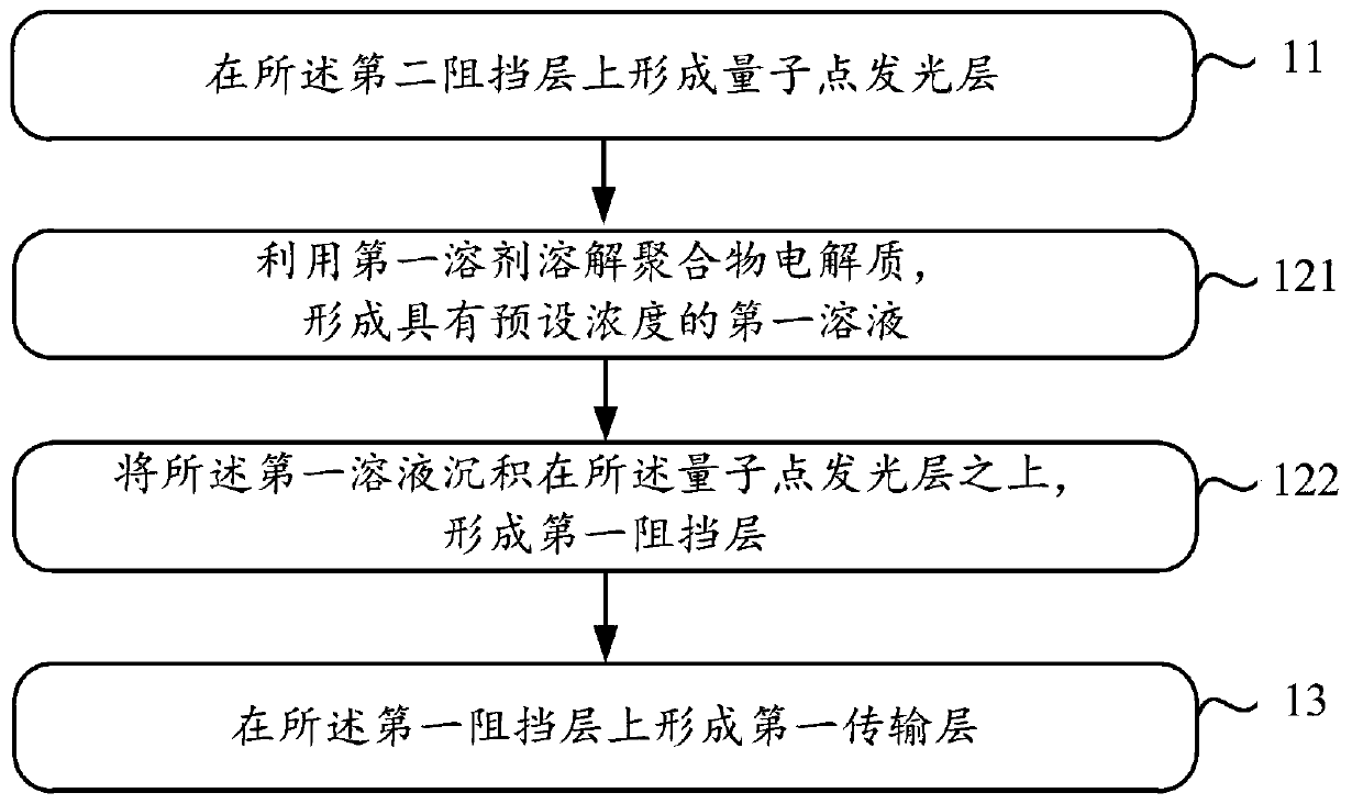
[0055] Based on the above-mentioned scheme, the manufacturing method of the QLED device provided by the embodiment of the present application, see image 3 shown, including:

[0056] Step 11: forming a quantum dot light-emitting layer.

[0057] Specifically, the method steps for forming the quantum dot light-emitting layer can be as shown in the above-mentioned embodiments, and will not be repeated here. The process of forming the first barrier layer in step 12 can be specifically implemented through the following steps 121 and 122 .

[0058] Step 121: Dissolving the polymer electrolyte with a first solvent to form a first solution with a preset concentration.

[0059] In this step, the first solvent used to dissolve the polymer electrolyte is determined; considering that the first barrier layer needs to be made on the quantum dot light-emitting layer, in order to avoid mutual solubility of solvents between adjacent film layers, it is necessary to When making the layer, the...

Embodiment 3

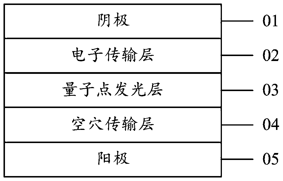
[0083] The film layer structure of the QLED device provided by the embodiment of the present application is as follows: Figure 6 As shown, it mainly includes: a quantum dot luminescent layer 61, a first transport layer 62 located on the quantum dot luminescent layer 61, and a second transport layer 62 located between the quantum dot luminescent layer 61 and the first transport layer 62 A barrier layer 63, the first barrier layer 63 includes a polymer electrolyte; wherein, the first barrier layer 63 is used to block at least part of the nanoparticles in the first transport layer 62 from leaking to the quantum dots to emit light Layer 61.

[0084] Considering that in this application, the first transport layer can be either an electron transport layer or a hole transport layer, then, when only the first barrier layer exists, the QLED device can include the following two structures:

[0085] Structure 1: The first transport layer is an electron transport layer.

[0086] like ...


PUM

PropertyMeasurementUnit
thicknessaaaaaaaaaa
thicknessaaaaaaaaaa

Abstract

This application involves the technology field of luminous devices, especially for a quantum dot -light diode QLED device and its production methods and devices to alleviate the nanoparticle leakage in the first transmission layer formed on the existing technology.The problem of affecting the performance of the quantum point luminous layer.This device includes: quantum dot luminous layer, the first transmission layer above the quantum dot luminous layer, the first blocking layer between the quantum dot luminous layer and the first transmission layer.At least part of the nanoparticle in the first transmission layer is leaked to the quantum dot luminous layer.Because the first blocking layer contains a dense mesh aggregation electrolyte, the first blocking layer can block at least part of the nanoparticle in the first transmission layer leak to the quantum dot luminous layer to avoid the first transmission layer and quantum dot.Mutual dissolving between the luminous layers to ensure the luminous performance of the luminous layer of the quantum dot.

Description

technical field [0001] The present application relates to the field of display technology, in particular to a quantum dot light emitting diode (QLED) device and a manufacturing method and device thereof. Background technique [0002] Quantum Dot Light Emitting Diodes (QLED) is a new type of self-luminous technology that does not require additional light sources. Quantum Dots are extremely small semiconductor nanoparticles that cannot be seen by the naked eye. particles with diameters ranging from a few nanometers to tens of nanometers. [0003] like figure 1 As shown, it is a schematic diagram of the film layer structure of the existing QLED device. In the film layer of the device, from bottom to top, it mainly includes: cathode 01, electron transport layer 02, quantum dot light-emitting layer 03, hole transport layer 04, anode 05 and other film layers. In addition, it may also include: an electron injection layer, a hole injection layer, etc., figure 1 not shown. [00...

Claims


Application Information

Patent Timeline
Patent Type & Authority Patents(China)
IPC IPC(8): H01L51/50H01L51/54H01L51/56H10K99/00
CPCH10K85/00H10K50/115H10K50/80H10K50/16H10K50/00H10K50/15H10K71/00H10K85/111H10K85/115H10K71/15H10K2102/331
Inventor 王建太邢汝博杨小龙刘会敏孙萍韦冬
Owner KUNSHAN NEW FLAT PANEL DISPLAY TECH CENT
Features
  • R&D
  • Intellectual Property
  • Life Sciences
  • Materials
  • Tech Scout
  • Unparalleled Data Quality
  • Higher Quality Content
  • 60% Fewer Hallucinations
Learn More