

Panchromatic micrometer LED display chip based ona gallium nitride nanopore array/quantum dot composite structure and preparation method thereof
A gallium nitride nanometer and nanohole array technology is applied in the field of full-color micron LED display chips and their preparation, which can solve the problems that restrict the development of micron LED display technology, the low quality of micron LED display chips, and the low color conversion efficiency of quantum dots, etc. problems, to achieve high transfer efficiency and yield, improve internal quantum efficiency and color conversion efficiency, and shorten manufacturing time.
- Summary
- Abstract
- Description
- Claims
- Application Information
AI Technical Summary
Problems solved by technology
Method used
Image

Examples
Embodiment 1
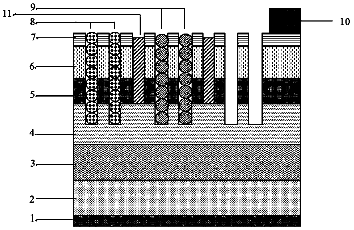
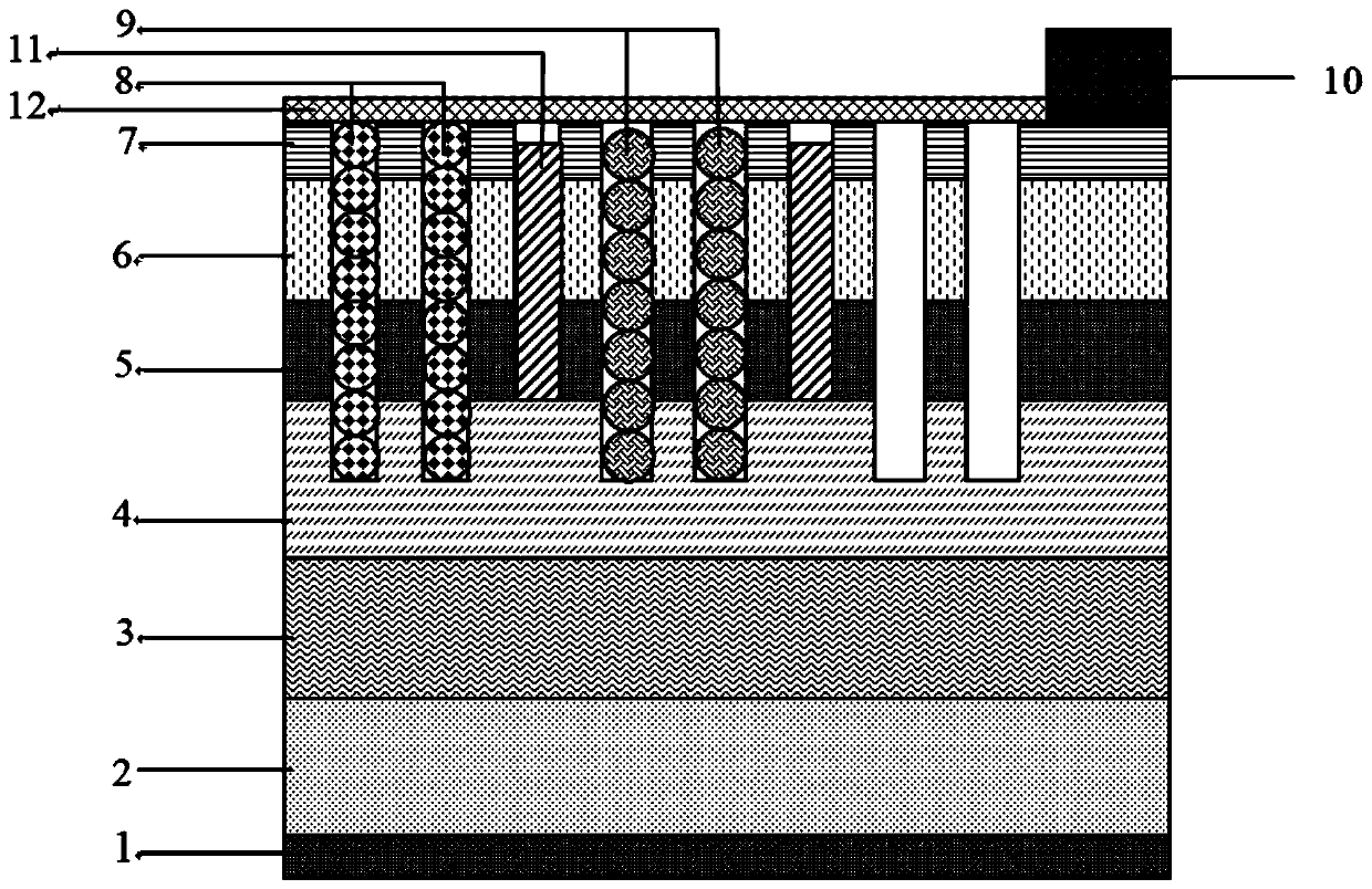
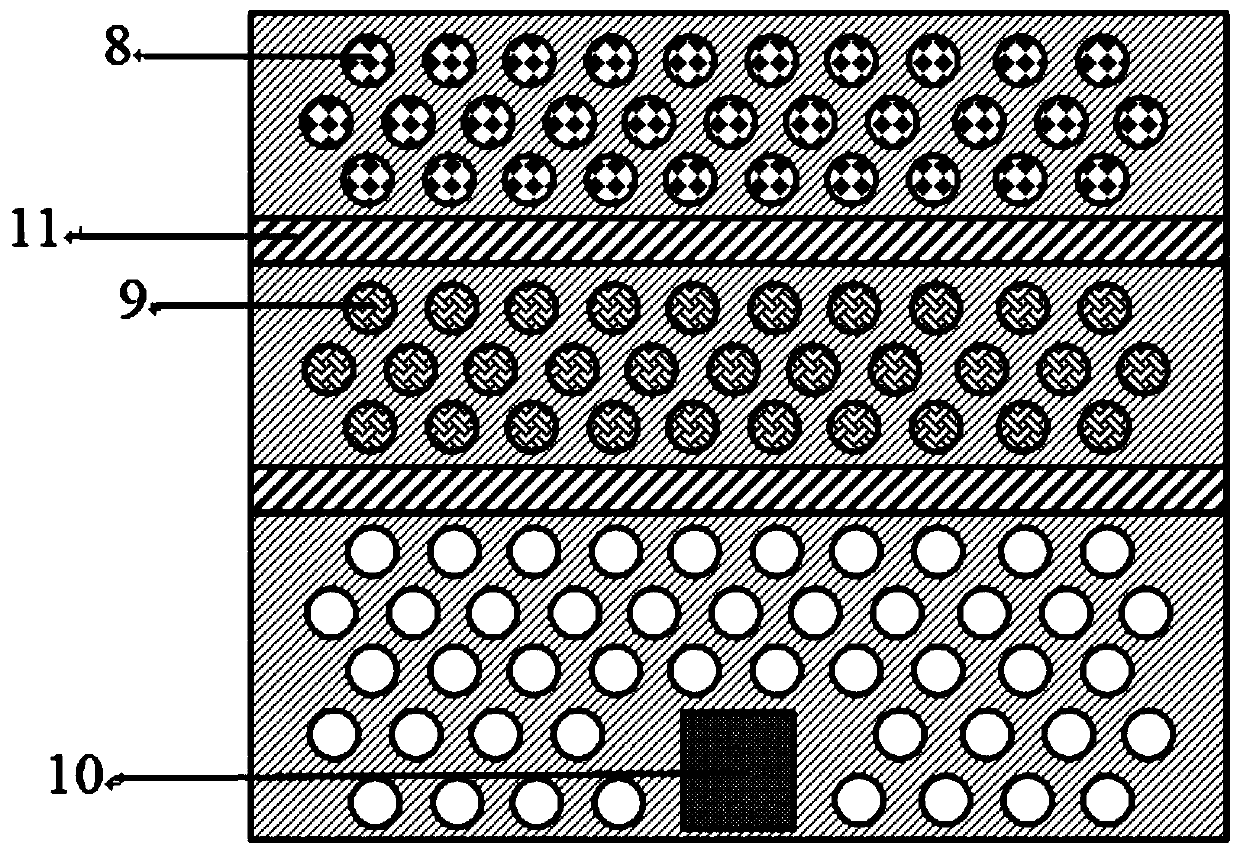
[0049] The preparation method of the hybrid RGB microhole LED array device based on Group III nitride semiconductor / quantum dots, the steps include:
[0050] (1) Select a suitable silicon substrate 2, after performing standard cleaning, use metal organic chemical vapor deposition (MOCVD) technology to sequentially grow a GaN buffer layer 3, an n-type GaN layer 4, and an undoped layer on the silicon substrate GaN multi-quantum well active layer 5, and a p-type GaN layer 6, as the blue LED epitaxial layer;
[0051] (2) Using plasma-enhanced chemical vapor deposition (PECVD) technology, a layer of 150nm thick SiO was evaporated on the GaN blue LED epitaxial wafer 2 Dielectric layer, PECVD grown SiO 2 The way is to pass 5% SiH into the reaction chamber 4 / N 2 and N 2 The mixed gas of O, the flow rates are 100sccm and 450sccm respectively, under the condition of pressure 300mTorr, power 10W, temperature 350℃, through SiH x +O→SiO 2 (+H 2 ) reaction to deposit SiO on the epit...
PUM
| Property | Measurement | Unit |
|---|---|---|
| Length | aaaaa | aaaaa |
| Depth | aaaaa | aaaaa |
| Width | aaaaa | aaaaa |
Abstract
Description
Claims
Application Information