Polishing process for cadmium-zinc-cadmium wafer

A cadmium zinc telluride wafer and process technology, applied in grinding/polishing equipment, manufacturing tools, working carriers, etc., can solve the problem of slow intermediate line speed of the wafer, inability to further improve the surface roughness, and unbalanced chip loss inside and outside the wafer, etc. problem, to achieve the effect of reducing workload, balancing the amount of polishing removal, and reducing defects

Inactive Publication Date: 2019-08-13
湖南大合新材料有限公司
View PDF7 Cites 3 Cited by
  • Summary
  • Abstract
  • Description
  • Claims
  • Application Information

AI Technical Summary

Problems solved by technology

However, there is still a problem in chemical mechanical polishing: the middle line speed of the wafer is slow, and the line speed increases as it gets closer to the outer edge, which causes the phenomenon of unbalanced internal and external drops of the wafer to always exist, so that the surface roughness of the product is always unsatisfactory. further improvement
According to reports, the surface roughness of existing CdZnTe wafers is usually above 1nm

Method used


Image

  • Polishing process for cadmium-zinc-cadmium wafer
  • Polishing process for cadmium-zinc-cadmium wafer

Examples


Embodiment Construction

[0018] The following examples are provided below to specifically describe the present invention. It is necessary to point out that the following examples are only used to further illustrate the present invention, and cannot be interpreted as limiting the protection scope of the present invention. Some non-essential improvements or adjustments made by the embodiments to the present invention still belong to the protection scope of the present invention.

[0019] In this embodiment, a CdZnTe wafer with a particle size of 3 cm, a thickness difference of 15 μm, and a flatness of 15 μm is used as an experimental sample.

[0020] A polishing process for a cadmium zinc telluride wafer, comprising the following steps:

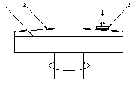
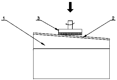
[0021] Step 1. Use an expanded glass disk with a particle size of 300mm. The surface of the glass disk is processed into a frosted surface by a striped ceramic disk, and the edge is processed into a D-shaped or T-shaped. The pressure during grinding is 0.9N / cm 2 , the...


PUM

PropertyMeasurementUnit
surface roughnessaaaaaaaaaa
particle diameteraaaaaaaaaa

Abstract

The invention discloses a polishing process for a cadmium-zinc-cadmium wafer. The polishing process comprises the following steps of grinding: grinding the cadmium-zinc-cadmium crystal by selecting afrosted puffed glass disc; milling: rotating a grinding wheel of a milling machine, removing a surface damage layer of the wafer, controlling the removal amount to be 80-150 microns and the surface roughness to be less than or equal to 20 nm, spraying cooling water between the wafer and the grinding wheel in the milling process, and transferring the wafer to a polishing procedure after processingis finished; and chemical-mechanical polishing: arranging the surface of a bearing disc to be in an inclined shape which is gradually lowered from the middle part of the disc to the circumference of the disc with an inclination angle to be 2 plus / minus 0.5 degrees, placing the cadmium-zinc-cadmium wafer on the bearing disc, adding a polishing solution with a pH value to be 9-11 in the chemical-mechanical polishing process, controlling a rotating speed of a grinding head to be 3-20r / min, the pressure to be 2-10N / cm2, the removal amount to be 20-40 microns and the time to be 20-40 min, and enabling the polishing solution to flow back and return to a polishing solution supply system after polishing is finished. The polishing process can effectively reduce scratches, scorings and cracks of thewafer, can reduce the surface roughness of the wafer and has a wide application prospect.

Description

technical field [0001] The invention relates to the technical field of wafer processing, in particular to a polishing process of cadmium zinc telluride. Background technique [0002] Cadmium zinc telluride crystal is a wide bandgap II-VI compound semiconductor, which has excellent photoelectric properties, and is by far the most ideal semiconductor material for the manufacture of room temperature X-ray and γ-ray detectors, and is widely used as the epitaxy of infrared detector HgCdTe Substrates and room temperature nuclear radiation detectors and other fields. In the existing CdZnTe wafer polishing process, the wafer is usually mechanically ground first and then chemically mechanically polished. During the mechanical grinding process, the material for making the grinding disc is usually ductile iron, which is easily oxidized to obtain ferric oxide Particles, resulting in wafer scratches, scratches, dark cracks. [0003] Chemical Mechanical Polishing (CMP) is a means of obt...

Claims


Application Information

Patent Timeline
Patent Type & Authority Applications(China)
IPC IPC(8): B24B1/00B24B37/10B24B37/30B24B57/02
CPCB24B1/00B24B37/10B24B37/30B24B57/02
Inventor 潘永志张明文陈琳
Owner 湖南大合新材料有限公司
Why Eureka
Try Eureka