Organic electroluminescent material and organic electroluminescent device containing material

An electroluminescent material and electroluminescent device technology, which is applied in the directions of luminescent materials, electro-solid devices, electrical components, etc., can solve the problems of excessive stacking, decreased device life, etc., to reduce device driving voltage, improve device efficiency and Life, increase in glass transition temperature and effect of vapor deposition temperature

Inactive Publication Date: 2019-08-16
SHAANXI LIGHTE OPTOELECTRONICS MATERIAL CO LTD
View PDF5 Cites 96 Cited by
  • Summary
  • Abstract
  • Description
  • Claims
  • Application Information

AI Technical Summary

Problems solved by technology

[0009] However, the stacking of fluorene and diphenylfluorene π-π molecules is too strong

Method used


Image

  • Organic electroluminescent material and organic electroluminescent device containing material
  • Organic electroluminescent material and organic electroluminescent device containing material
  • Organic electroluminescent material and organic electroluminescent device containing material

Examples


Embodiment 1

[0095] Embodiment 1: blue organic electroluminescent device

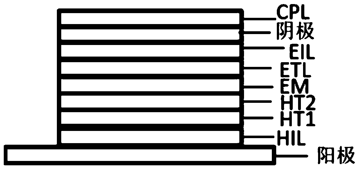
[0096] The anode was prepared by the following process: the thickness was The ITO substrate (manufactured by Corning) was cut into a size of 40mm×40mm×0.7mm, and it was prepared into an experimental substrate with cathode, anode and insulating layer patterns by photolithography process, and the surface was treated by ultraviolet ozone and O2:N2 plasma , to increase the work function of the anode (experimental substrate) and remove scum.

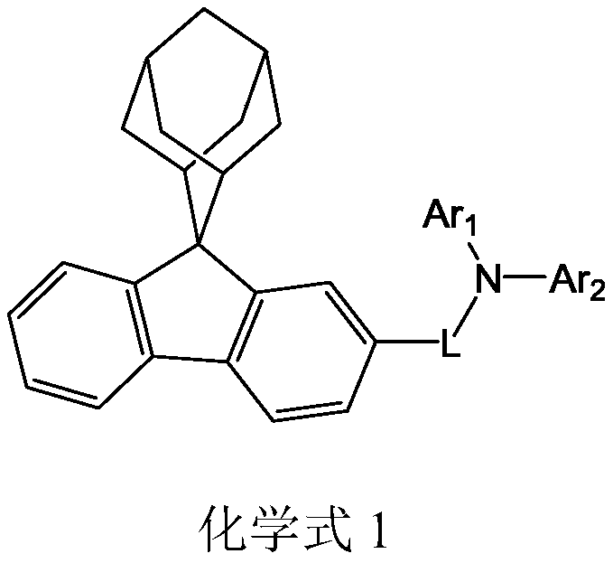
[0097] Vacuum evaporated m-MTDATA on the experimental substrate (anode) to form a thickness of The hole injection layer (HIL), and compound 1 is vacuum evaporated on the hole injection layer to form a thickness of The first hole transport layer (HT1).

[0098] Evaporate TCTA on the first hole transport layer to form a thickness of The second hole transport layer (HT2).

[0099] Using α,β-AND as the main body and doping 4,4'-(3,8-diphenylpyrene-1,6-diylbis(N,N-diphenylanili...

Embodiment 2-5

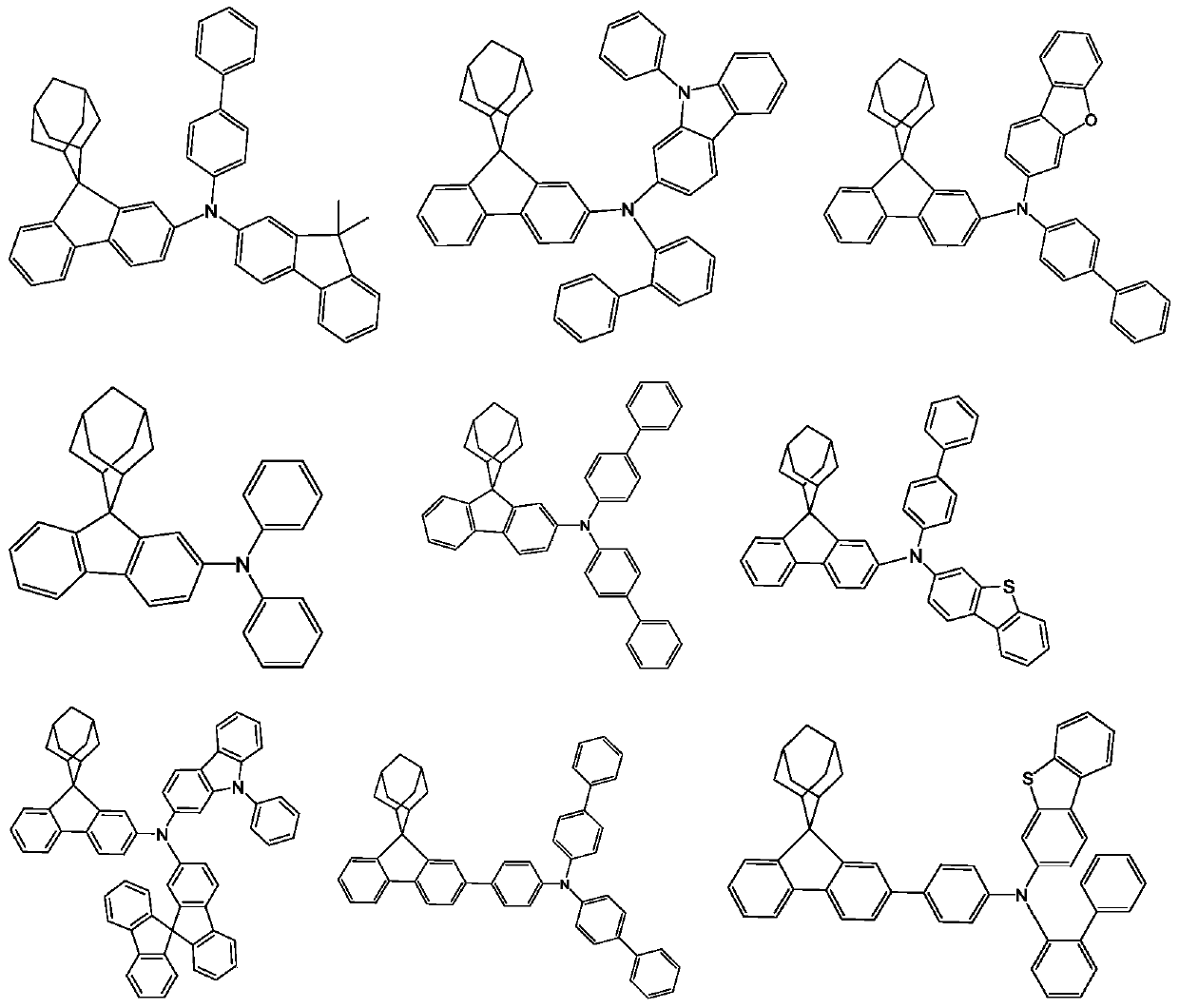
[0103] An organic electroluminescent device was fabricated by the same method as in Example 1 except that the compounds shown in Table 1 were each used when forming the first hole transport layer (HT1).

[0104] That is, Example 2 uses Compound 2 to make an organic electroluminescent device, Example 3 uses Compound 3 to make an organic electroluminescent device, Example 4 uses Compound 4 to make an organic electroluminescent device, and Example 5 uses Compound 5 to make an organic electroluminescent device. Light-emitting device, the device performance is shown in Table 1.

Embodiment 6

[0116] Embodiment 6: red organic electroluminescent device

[0117] The anode was prepared by the following process: the thickness was The ITO substrate (manufactured by Corning) was cut into a size of 40mm × 40mm × 0.7mm, and it was prepared into an experimental substrate with cathode, anode and insulating layer patterns by using a photolithography process, using ultraviolet ozone and O 2 :N 2 Plasma surface treatment was performed to increase the work function of the anode (experimental substrate) and to remove scum.

[0118] Vacuum vapor-deposit m-MTDATA on the experimental substrate (anode) to form a thickness of The hole injection layer (HIL), and NPB is evaporated on the hole injection layer to form a thickness of The first hole transport layer (HT1).

[0119] Compound 6 is vacuum evaporated on the first hole transport layer to form a thickness of The second hole transport layer (HT2).

[0120] Evaporate 4,4'-N,N'-dicarbazole-biphenyl (referred to as "CBP") as ...


PUM


Abstract

The invention provides an organic electroluminescent material and an organic electroluminescent device containing the material. The material has a structural formula shown in the description. The material provided by the invention is used as a hole transporting layer, a hole injecting layer or an electron blocking layer of the organic electroluminescent device, so that the organic electroluminescent device has a lower driving voltage, higher luminous efficiency, and a better service life.

Description

technical field [0001] The invention belongs to the technical field of electroluminescence, and relates to an organic electroluminescence material and an organic electroluminescence device containing the material. Background technique [0002] In recent years, an organic electroluminescent device (OLED, Organic electroluminescent device) as a new generation display technology has gradually entered people's field of vision. A common organic electroluminescent device is composed of an anode, a cathode, and more than one organic layer arranged between the cathode and the anode. When a voltage is applied to the cathode and anode, the two electrodes generate an electric field. Under the action of the electric field, the electrons on the cathode side move to the light-emitting layer, and the electrons on the anode side also move to the light-emitting layer. The two combine to form excitons in the light-emitting layer, and the excitons are excited. The state releases energy outwar...

Claims


Application Information

Patent Timeline
IPC IPC(8): C07C211/54C07C211/61C07D209/88C07D307/91C07D333/76C09K11/06H01L51/54
CPCC07C211/61C07D209/88C07D307/91C07D333/76C07C211/54C09K11/06C07C2603/94C07C2603/18C09K2211/1007C09K2211/1011C09K2211/1014C09K2211/1029C09K2211/1088C09K2211/1092H10K85/636H10K85/626H10K85/633H10K85/631H10K85/6576H10K85/6574H10K85/6572
Inventor 马天天聂齐齐李红燕冯震沙荀姗王亚龙孙占义
Owner SHAANXI LIGHTE OPTOELECTRONICS MATERIAL CO LTD
Why Eureka
Try Eureka