Solar cell, preparation method thereof and photovoltaic module

A solar cell and electrode technology, which is applied in the field of solar cells, can solve the problems of limiting the efficiency of solar cells, the small size of polysilicon thin films, and the difficulty of polysilicon thin films, and achieve the effects of reducing production costs, increasing the lifetime of minority carriers, and improving efficiency

Pending Publication Date: 2019-08-20
JA SOLAR TECH YANGZHOU +1
View PDF10 Cites 4 Cited by
  • Summary
  • Abstract
  • Description
  • Claims
  • Application Information

AI Technical Summary

Problems solved by technology

However, due to the small particles and many intercrystals of the polysilicon film, it is difficult to obtain a higher doping concentration for the polysilicon film, which limits the improvement of the efficiency of solar cells.

Method used


Image

  • Solar cell, preparation method thereof and photovoltaic module
  • Solar cell, preparation method thereof and photovoltaic module
  • Solar cell, preparation method thereof and photovoltaic module

Examples


preparation example Construction

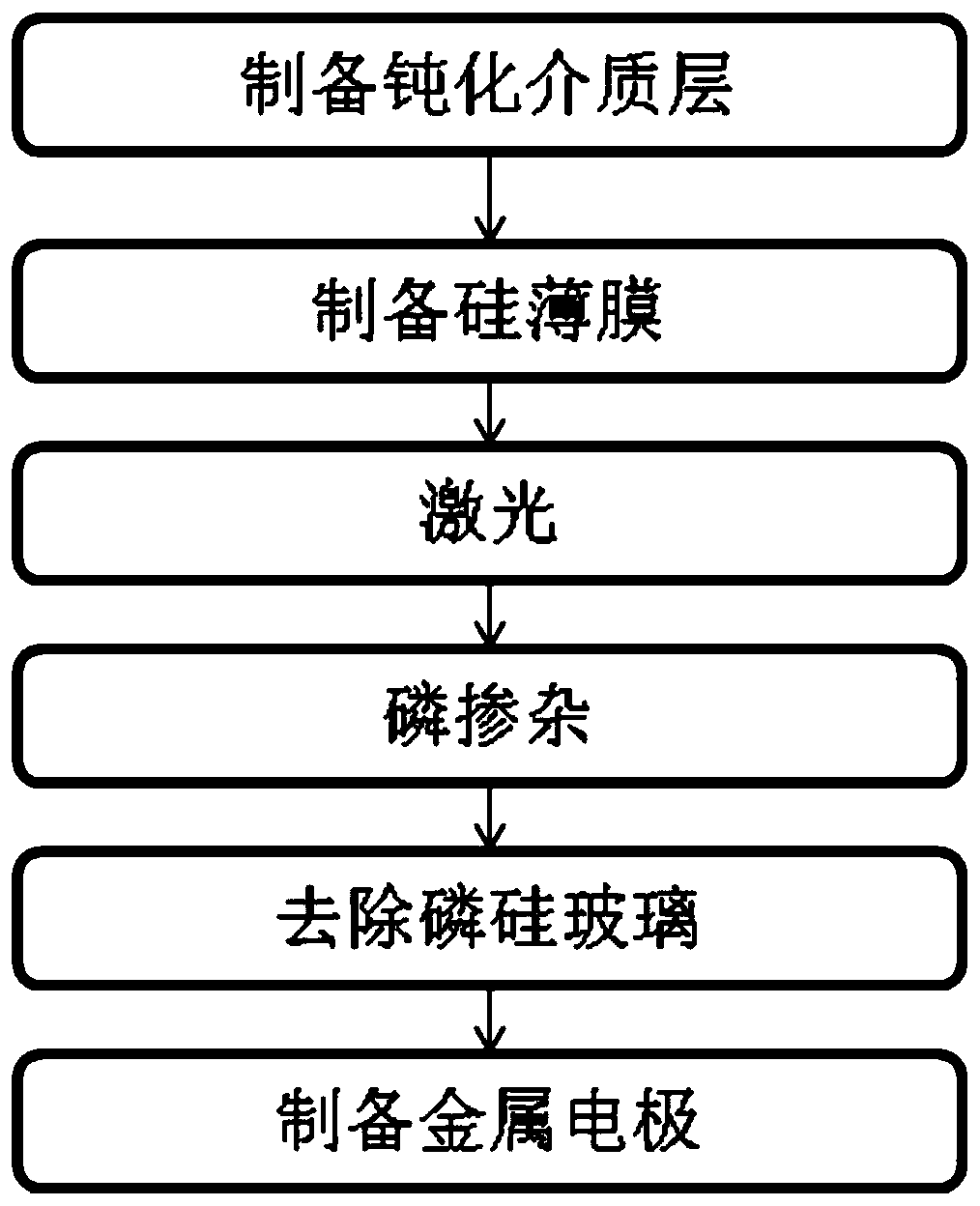
[0100] The present invention also provides the preparation method of the above-mentioned solar cell, such as figure 2 Shown, this preparation method comprises the following steps:

[0101] S1: providing a silicon substrate 1;

[0102] S2, setting a passivation dielectric layer 4 on the silicon substrate 1;

[0103] S3: setting a semiconductor thin film on the passivation medium layer 4;

[0104] S4: removing the semiconductor thin film and the passivation medium layer 4 at the predetermined position to expose a part of the surface of the silicon substrate 1;

[0105] S5: Doping the area exposed on the surface of the silicon base 1 to form a doped area 2 in the area exposed on the surface of the silicon base 1, and the area covered by the semiconductor film and the passivation medium layer 4 on the surface of the silicon base 1 is the non-doped area 3 ;

[0106] S6: forming the electrode 6 in contact with the doped region 2 .

[0107] In the preparation method of the pres...

Embodiment 1

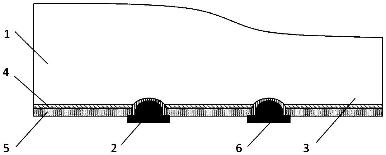
[0120] like figure 1 As shown, the N-type solar cell provided in this embodiment is an N-type solar cell with local doping of the silicon substrate, including an N-type silicon substrate 1, and a partially doped region 2 and a non-doped silicon substrate are provided on the back side of the N-type silicon substrate 1. The impurity area 3 is provided with a passivation medium layer 4 on the surface of the non-doped area 3 of the silicon substrate 1, a doped silicon film is provided on the passivation medium layer 4, and an electrode is provided on the partially doped area 2. 6.

[0121] The surface of the N-type silicon substrate 1 is a textured surface.

[0122] The doped regions 2 and the non-doped regions 3 on the silicon substrate 1 are distributed alternately.

[0123] The doped silicon film is specifically a doped amorphous silicon film with a thickness of 200 nm, and the doping element is the same as that of the local doping region 2 , and the doping element is phospho...

Embodiment 2

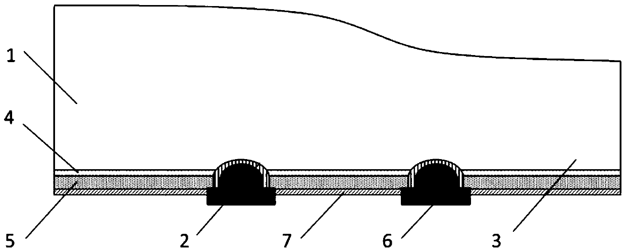
[0136] like image 3 As shown, the N-type solar cell provided in this embodiment is an N-type solar cell with local doping of the silicon substrate, including an N-type silicon substrate 1, and one of the surfaces of the N-type silicon substrate 1 is provided with a local doping region 2 and The non-doped region 3 is provided with a passivation medium layer 4 on the surface of the non-doped region 3 of the silicon substrate 1, and a doped silicon film 5 is provided on the passivation medium layer 4, and the doped silicon film 5 and A silicon nitride film 7 is provided on the partially doped region 2 of the silicon substrate 1 , and a metal contact electrode 6 is provided above the partially doped region 2 of the silicon substrate 1 .

[0137] The metal contact electrode 6 is disposed on the silicon nitride film 7 and corresponds to the position of the local doped region 2 .

[0138] Partially doped regions 2 and non-doped regions 3 of the silicon substrate 1 are distributed a...


PUM


Abstract

The invention discloses a solar cell, a preparation method thereof and a photovoltaic module. The solar cell comprises a silicon substrate (1), wherein a local region on the surface of the silicon substrate (1) is a doped region (2), and a region outside the doped region (2) is a non-doped region (3); a passivation medium layer (4) which is arranged on the non-doped region (3); a semiconductor thin film layer (5) which is arranged on the passivation medium layer (4); and an electrode (6) which is in contact with the doped region (2). According to the invention, the passivation dielectric layerand the doped silicon thin film are used for surface passivation of the surface of the non-doped region of a local back field cell, so that the passivation effect of the solar cell can be improved. The preparation method of the solar cell provided by the invention is compatible with the existing process, and is low in cost.

Description

[0001] This application claims the priority of the Chinese patent application submitted to the State Intellectual Property Office of China on November 27, 2018, with the application number 201811427296.X and the title of the invention "a solar cell and its preparation method, and a photovoltaic module", all of which The contents are incorporated by reference in this application. technical field [0002] The invention belongs to the technical field of solar cells, and in particular relates to a solar cell, a preparation method thereof, and a photovoltaic module. Background technique [0003] In order to obtain high-efficiency solar cells, the surface must have good passivation and low surface recombination rate, so that higher opening voltage, current and efficiency can be obtained. Due to the high surface concentration of the doped silicon substrate, the effect of passivating the doped silicon substrate is not very good, and the passivation of the undoped silicon substrate w...

Claims


Application Information

Patent Timeline
Patent Type & Authority Applications(China)
IPC IPC(8): H01L31/0216H01L31/02H01L31/068H01L31/18
CPCH01L31/02167H01L31/1804H01L31/1868H01L31/02008H01L31/068Y02E10/547Y02P70/50
Inventor 张俊兵黄卓汤坤
Owner JA SOLAR TECH YANGZHOU
Why Eureka
Try Eureka