A Nonpolar Algan-based Schottky UV Detector

A non-polar, detector technology, used in semiconductor devices, electrical components, circuits, etc., can solve the problems of large dark current, lattice mismatch, poor signal-to-noise ratio and stability of ultraviolet detectors

Active Publication Date: 2021-03-09
SOUTHEAST UNIV
View PDF7 Cites 0 Cited by
  • Summary
  • Abstract
  • Description
  • Claims
  • Application Information

AI Technical Summary

Problems solved by technology

[0004] However, if image 3 In the traditional polar AlGaN-based Schottky UV detector shown, due to the presence of a polarized electric field with an intensity as high as MV / cm in the direction parallel to the incident light, the photogenerated carriers in the ohmic contact layer are perpendicular to The lateral movement of the polarization electric field to the corresponding electrode will be strongly hindered by the polarization electric field, so that the photoelectric conversion efficiency of the detector is not high
In addition, during the growth process of high Al composition AlGaN materials, the large lattice mismatch and thermal mismatch with the substrate material will also introduce a large number of dislocations and defects that usually serve as conductive channels
Moreover, defects existing at the metal-semiconductor interface can easily lead to the formation of tunneling current
The above-mentioned problems cause the dark current of the existing Schottky UV detector to be large, and the signal-to-noise ratio and stability are poor, which seriously limits the performance and development of the Schottky UV detector.

Method used


Image

  • A Nonpolar Algan-based Schottky UV Detector
  • A Nonpolar Algan-based Schottky UV Detector
  • A Nonpolar Algan-based Schottky UV Detector

Examples


Embodiment 1

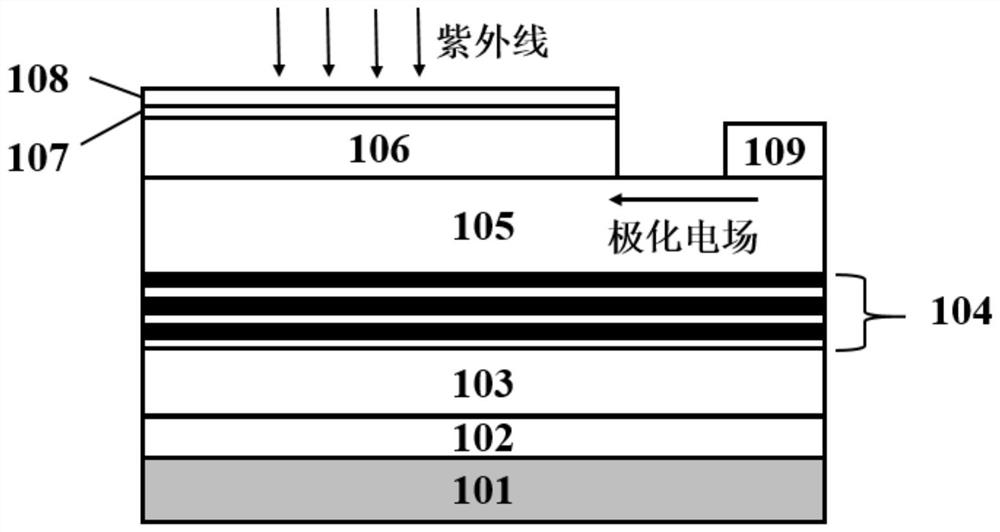
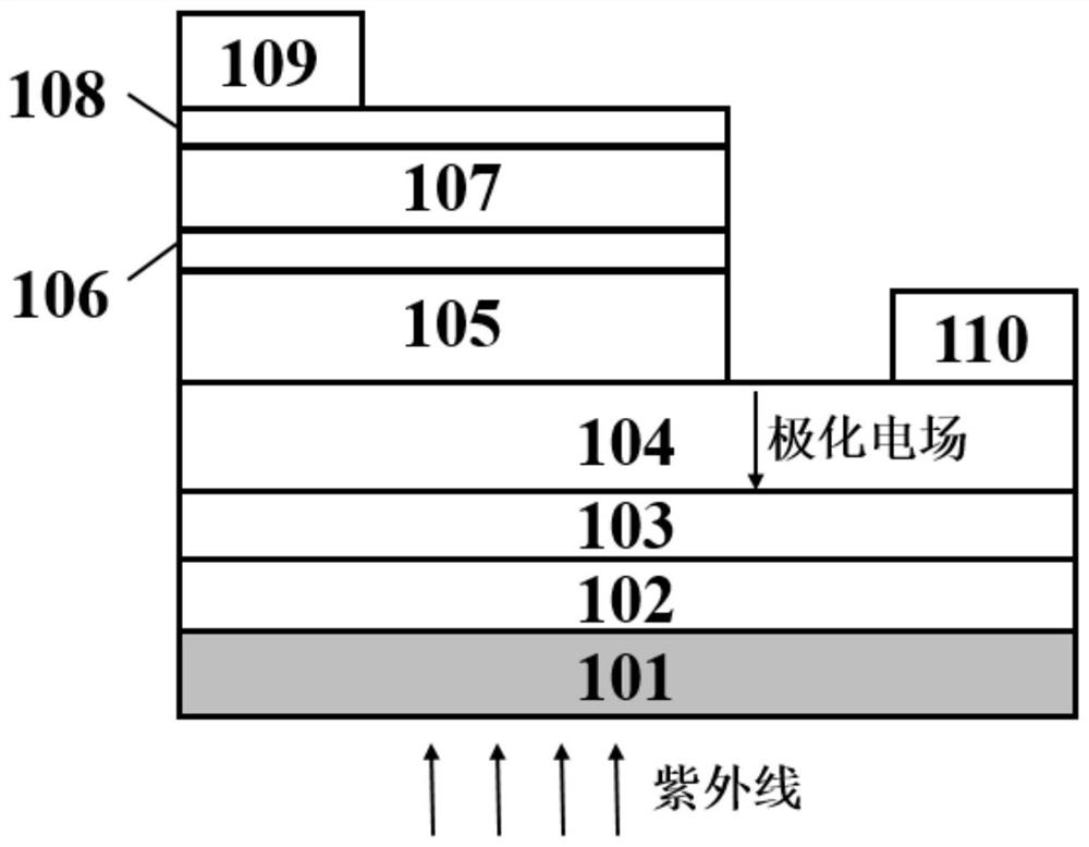
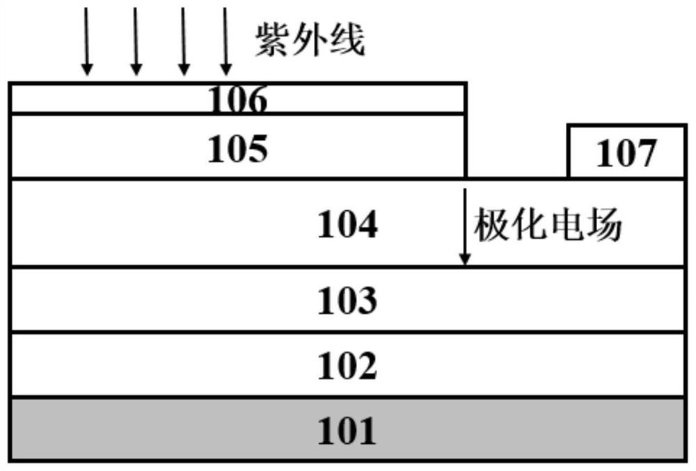
[0018] figure 1 Shown is a non-polar AlGaN-based Schottky ultraviolet detector provided by the present invention, including a substrate (101), a low-temperature AlN nucleation layer (102), and a high-temperature AlN buffer layer (103) arranged in sequence from bottom to top , AlN / Al 0.6 Ga 0.4 N superlattice structure (104), n-type doped n-Al 0.3 Ga 0.7 N layer (105), n-type doped n-Al 0.38 Ga 0.62 N absorption layer (106), AlN barrier enhancement layer (107), metal thin film layer (108), in n-Al 0.3 Ga 0.7 Ohmic electrodes (109) are drawn out from the N layer (105). Except for the substrate (101), metal thin film layer (108) and ohmic electrode (109), all other layers are made of non-polar AlGaN base material.

[0019] The metal thin film layer (108) and the ohmic electrode (109) are respectively located at the negative and positive poles of the transverse polarization electric field.

[0020] The material of the metal thin film layer (108) is Au, and its work funct...

Embodiment 2

[0028] figure 1 Shown is a non-polar AlGaN-based Schottky ultraviolet detector provided by the present invention, including a substrate (101), a low-temperature AlN nucleation layer (102), and a high-temperature AlN buffer layer (103) arranged in sequence from bottom to top , AlN / Al 0.6 Ga 0.4 N superlattice structure (104), n-type doped n-Al 0.3 Ga 0.7 N layer (105), n-type doped n-Al 0.38 Ga 0.62 N absorption layer (106), AlN barrier enhancement layer (107), metal thin film layer (108), in n-Al 0.3 Ga 0.7 Ohmic electrodes (109) are drawn out from the N layer (105). Except for the substrate (101), metal thin film layer (108) and ohmic electrode (109), all other layers are made of non-polar AlGaN base material.

[0029] The metal thin film layer (108) and the ohmic electrode (109) are respectively located at the negative and positive poles of the transverse polarization electric field.

[0030] The material of the metal thin film layer (108) is Au, and its work funct...

Embodiment 3

[0035] figure 1 Shown is a non-polar AlGaN-based Schottky ultraviolet detector provided by the present invention, including a substrate (101), a low-temperature AlN nucleation layer (102), and a high-temperature AlN buffer layer (103) arranged in sequence from bottom to top , AlN / Al 0.6 Ga 0.4 N superlattice structure (104), n-type doped n-Al 0.3 Ga 0.7 N layer (105), n-type doped n-Al 0.38 Ga 0.62 N absorption layer (106), AlN barrier enhancement layer (107), metal thin film layer (108), in n-Al 0.3 Ga 0.7 Ohmic electrodes (109) are drawn out from the N layer (105). Except for the substrate (101), metal thin film layer (108) and ohmic electrode (109), all other layers are made of non-polar AlGaN base material.

[0036] The metal thin film layer (108) and the ohmic electrode (109) are respectively located at the negative and positive poles of the transverse polarization electric field.

[0037] The material of the metal thin film layer (108) is Au, and its work funct...


PUM

PropertyMeasurementUnit
thicknessaaaaaaaaaa
thicknessaaaaaaaaaa
thicknessaaaaaaaaaa

Abstract

The present invention provides a non -polar Algan Krutki UV detector. From bottom to top to set up substrate, low -temperature aln nuclear layer, high temperature Aln buffer layer, Aln / Al x GA 1‑x N -ultra -crystal structure, N -type doped N‑al y GA 1‑y N layer, N -type doped n 、al z GA 1‑z N absorbing layer, ALN potential barrier enhancement layer, metal film layer, in N‑al y GA 1‑y The n layer leads the Ohm electrode, where 0 <y <z <x <1.Due to non -polar N‑al y GA 1‑y There is a horizontal polarized electric field that points to cathode in the n layer, so it will speed up the photochemical carrier in N‑al y GA 1‑y The N layer migrates to the EME, thereby greatly improving the production efficiency of the optical current, thereby improving the optoelectronic conversion efficiency and response of the device.Insert aln / al x GA 1‑x N -ultra -crystal structure, while increasing the height of the buffer layer, improve the crystal quality of the Algan extension layer.In N‑al z GA 1‑z N The enhanced layer of the ALN Blood of the absorbing layer and the metal film layer can effectively increase the height and thickness of the Schartki Blood.Therefore, aln / al x GA 1‑x The insertion of the N -ultra -lattice structure and the ALN potential barrier enhanced layer is conducive to reducing the dark current of the device and improving the signal -to -noise ratio and stability of the detector.

Description

technical field [0001] The invention relates to the field of semiconductor optoelectronic devices, in particular to a non-polar AlGaN-based Schottky ultraviolet detector. Background technique [0002] With the vigorous development of third-generation semiconductor materials such as GaN, diamond and SiC, it will lay the foundation for the development of high-performance ultraviolet detectors. Especially AlGaN material, because its forbidden band width can be adjusted between 3.4-6.2 eV by controlling the aluminum composition, and the corresponding spectral wavelength covers the ultraviolet region of 365-200 nm, so it has significant advantages in ultraviolet detection. It is an ideal material for making ultraviolet photodetection devices. [0003] At present, most of the ultraviolet detectors used in the market are such as figure 2 The p-n junction or pin structure shown is usually back-illuminated. Compared with these traditional UV detectors, Schottky UV detectors have u...

Claims


Application Information

Patent Timeline
Patent Type & Authority Patents(China)
IPC IPC(8): H01L31/0304H01L31/108
CPCH01L31/03044H01L31/03048H01L31/108Y02E10/544
Inventor 张雄饶立锋崔一平
Owner SOUTHEAST UNIV
Why Eureka
Try Eureka