A kind of array substrate and preparation method thereof

A technology of array substrates and substrate substrates, which is applied in semiconductor/solid-state device manufacturing, semiconductor/solid-state device components, semiconductor devices, etc., can solve the problems of H element affecting device performance, energy consumption and high cost, and achieve stable performance, The effect of low energy consumption

Active Publication Date: 2020-10-16
TCL CHINA STAR OPTOELECTRONICS TECH CO LTD
View PDF6 Cites 0 Cited by
  • Summary
  • Abstract
  • Description
  • Claims
  • Application Information

AI Technical Summary

Problems solved by technology

[0004] The present application provides an array substrate and a preparation method thereof, which can solve the problems of high energy consumption and high cost when preparing a passivation layer on the substrate substrate of the existing IGZO TFT, and the problem that H element easily enters the IGZO film layer and affects the performance of the device.

Method used


Image

  • A kind of array substrate and preparation method thereof
  • A kind of array substrate and preparation method thereof
  • A kind of array substrate and preparation method thereof

Examples


Embodiment Construction

[0029] The following descriptions of the various embodiments refer to the accompanying drawings to illustrate specific embodiments that the present application can be used to implement. The directional terms mentioned in this application, such as [top], [bottom], [front], [back], [left], [right], [inside], [outside], [side], etc., are for reference only The orientation of the attached schema. Therefore, the directional terms used are used to illustrate and understand the application, but not to limit the application. In the figures, structurally similar elements are denoted by the same reference numerals.

[0030] The present application aims at the technical problems that the existing IGZO TFT substrate has high energy consumption and cost when preparing the passivation layer, and H element is easy to enter the IGZO film layer and affect the performance of the device. This embodiment can solve this defect.

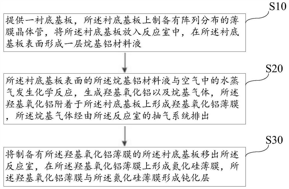
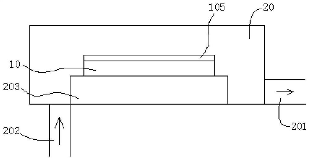
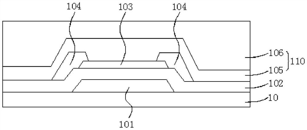
[0031] Such as figure 1 As shown in FIG. 2 , it is a flow chart o...


PUM


Abstract

The invention provides an array substrate and a preparation method thereof. According to the method, a layer of alkyl aluminum material solution is formed on the surface of a substrate with a thin film transistor; the alkyl aluminum material solution is subjected to a chemical reaction with water vapor to generate hydroxyl aluminum oxide and alkyl gas; the hydroxyl aluminum oxide is attached to the substrate to form a hydroxyl aluminum oxide film; the alkyl gas is discharged through a gas extraction system of a reaction chamber; and then a silicon nitride film is formed on the hydroxyl aluminum oxide film, so that a passivation layer of a composite structure of the hydroxyl aluminum oxide film and the silicon nitride film is formed. The hydroxyl aluminum oxide film is adopted to replace asilicon dioxide film in a conventional passivation layer, so that the energy consumption and the cost are relatively low, and the problem that the performance of a device is influenced due to the factthat an H element enters an indium gallium zinc oxide semiconductor layer can be solved.

Description

technical field [0001] The present application relates to the field of display technology, in particular to an array substrate and a preparation method thereof. Background technique [0002] Due to its high carrier mobility, IGZO (Indium Gallium Zinc Oxide) is considered to be an ideal semiconductor layer material in next-generation TFT devices. However, IGZO itself is unstable, and contact with H2O, O2, and excessive doping of H elements will deteriorate the performance of IGZO thin films. Therefore, the PV layer (passivation layer) of IGZO at this stage often adopts a double-layer structure of SiO2+SiNx. At present, SiO2 thin films are mainly prepared by CVD method; CVD film formation has a series of problems such as expensive equipment and high energy consumption (vacuumizing, heating). What is more worth mentioning is that in the existing film formation process (SiH4+N2O), the H element in silane can easily enter the IGZO film layer, thereby affecting the device perform...

Claims


Application Information

Patent Timeline
Patent Type & Authority Patents(China)
IPC IPC(8): H01L21/56H01L23/00H01L23/29H01L21/84H01L27/12
CPCH01L21/56H01L23/291H01L23/564H01L27/1214H01L27/1259
Inventor 彭钊
Owner TCL CHINA STAR OPTOELECTRONICS TECH CO LTD
Why Eureka
Try Eureka