A two-dimensional material phase-change memory cell

A two-dimensional material and storage unit technology, which is applied in the field of microelectronics, can solve the problems of low electrothermal efficiency and large thermal stress of phase change storage units, and achieve the goals of improving life, erasing times, reducing stress and strain, and high elastic coefficient Effect

Active Publication Date: 2021-10-08
HUAZHONG UNIV OF SCI & TECH
View PDF4 Cites 0 Cited by
  • Summary
  • Abstract
  • Description
  • Claims
  • Application Information

AI Technical Summary

Problems solved by technology

[0004] In view of the defects of the prior art, the purpose of the present invention is to provide a two-dimensional material phase-change memory unit, which aims to solve the problems of low electrothermal efficiency and large thermal stress of the phase-change memory unit

Method used


Image

  • A two-dimensional material phase-change memory cell
  • A two-dimensional material phase-change memory cell
  • A two-dimensional material phase-change memory cell

Examples


Embodiment 1

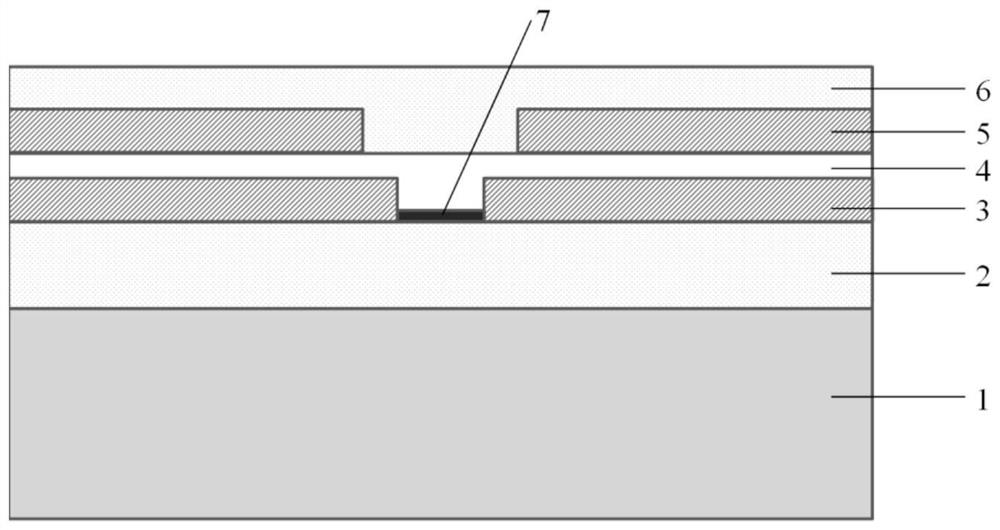
[0035] Such as figure 1 As shown, the present invention provides a two-dimensional material phase-change memory unit, including a substrate 1, a lower electrode 2, a first insulating layer 3, a phase-change layer 4, a second An insulating layer 5 , an upper electrode 6 , and a two-dimensional material layer 7 , wherein the two-dimensional material layer 7 is disposed on the contact surface between the phase change layer 4 and the lower electrode 2 .

[0036] Specifically, the substrate 1 may be a silicon single wafer substrate or other semiconductor material substrates.

[0037] Specifically, the lower electrode 2 is a conductive material that requires low resistivity and stable properties, and materials such as TiW, TiN, HfN, Ag, Al, Cu, W, Ta, and Pt can be used. The lower electrode can be made of the same material as the lower electrode 2 .

[0038] Specifically, the first insulating layer 3 is an insulating material, which requires high resistivity, low thermal conductiv...

Embodiment 2

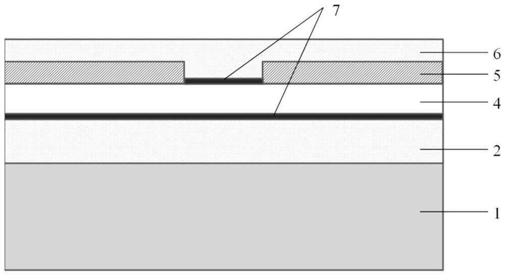
[0042] Different from the T-shaped structure of the embodiment, embodiment 2 provides a phase-change memory unit with a layered structure, such as figure 2 As shown, the difference lies in the structure of the phase change layer 4 and the two-dimensional material layer 7 is disposed between the upper electrode 6 and the lower electrode 2 and the phase change layer 4 at the same time.

Embodiment 3

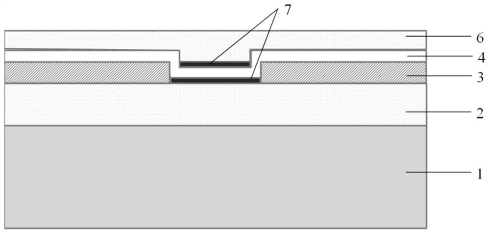
[0044] Such as image 3 As shown, a phase-change memory cell with a trench structure is provided, the difference lies in the structure of the phase-change layer 4 and the two-dimensional material layer 7 is disposed between the upper electrode 6 and the lower electrode 2 and the phase-change layer 4 at the same time.

[0045] Figure 4 to Figure 9 The specific preparation process of the two-dimensional material phase-change memory unit of Example 1 is shown:

[0046] Step 1: On a clean and dry silicon substrate 1, a lower electrode TiW thin film is prepared by magnetron sputtering. The thickness of the lower electrode 2 is 100 nm, and the width of the lower TiW electrode 2 is controlled to 15 um by photolithography technology. The method for preparing the TiW lower electrode 2 can be selected from one of sputtering, evaporation, chemical vapor deposition, and plasma enhanced chemical vapor.

[0047] Step 2: A molybdenum disulfide thin film is grown on the surface of the lower ...


PUM

PropertyMeasurementUnit
thicknessaaaaaaaaaa
thicknessaaaaaaaaaa
thicknessaaaaaaaaaa

Abstract

The invention discloses a two-dimensional material phase-change storage unit, which includes a substrate, a lower electrode, a phase-change layer, an upper electrode, and a two-dimensional material layer arranged sequentially above the substrate from bottom to top, and the two-dimensional material layer is arranged The contact surface between the phase change layer and the lower electrode is also arranged on the contact surface between the phase change layer and the upper electrode. The two-dimensional material used in the present invention has a very small thermal conductivity. In addition to the thermal resistance formed by the interface, it can also reduce the loss of heat, reduce the writing current, and improve the electrothermal efficiency; the two-dimensional material layer also has a good Excellent mechanical properties, such as high modulus of elasticity, high compressive strength and breaking strength, etc., can play a buffer role. During the phase change process, the thermal expansion and extrusion stress and strain of the phase change layer are smaller, so it can effectively reduce The stress and strain between the phase change layer and the electrode layer during the temperature rise of the small phase change can improve the life of the device and the number of times of erasing and writing.

Description

technical field [0001] The invention belongs to the technical field of microelectronics, and more specifically relates to a two-dimensional material phase-change memory unit. Background technique [0002] Under the circumstances that the capacity and storage speed of traditional memory are difficult to meet the needs of the new era, phase change memory has become a popular research object in the world due to its advantages of high read and write speed, high data retention, small cell size and non-volatility. , is considered to be the storage device most likely to replace flash memory. [0003] The working principle of phase change memory is based on the huge resistance difference between phase change materials in the crystalline state and the amorphous state, in which the crystalline state shows low resistance, and the amorphous state shows high resistance, which can respectively represent binary states "0", " 1". When the phase change memory is working, an electric pulse ...

Claims


Application Information

Patent Timeline
Patent Type & Authority Patents(China)
IPC IPC(8): H01L45/00
CPCH10N70/231H10N70/8616
Inventor 程晓敏温敏吴文豪缪向水
Owner HUAZHONG UNIV OF SCI & TECH
Why Eureka
Try Eureka