Forming method and product of multilevel microstructure on metal surface

A metal surface and microstructure technology, which is applied in the improvement of process efficiency, additive manufacturing, additive processing, etc., can solve the problems of poor repeatability, low preparation efficiency, easy to be damaged, etc. The process is simple and avoids the effect of easy destruction

Active Publication Date: 2021-01-05
HUAZHONG UNIV OF SCI & TECH
View PDF8 Cites 0 Cited by
  • Summary
  • Abstract
  • Description
  • Claims
  • Application Information

AI Technical Summary

Problems solved by technology

However, most of the above-mentioned surface microstructure preparation methods have the following problems: (1) they are selective to forming materials and have poor material adaptability; (2) the prepared microstructures are disordered or irregular, and it is difficult to effectively control the microstructure morphology; (3) The preparation process has gone through many processes, and the preparation efficiency is low; (4) The prepared microstructure is affected by many factors such as the material environment temperature, humidity, surface material components, etc., and the repeatability is poor; The processing and preparation costs are expensive, the environmental hazards are great, and more importantly, the surface adhesion strength of the microstructure substrate prepared by most methods is low, and the mechanical strength itself is low. , impact, etc.) are easily destroyed, and the practical application effect is poor, which leads to the extremely limited application range of the above microstructure preparation method

Method used


Image

  • Forming method and product of multilevel microstructure on metal surface
  • Forming method and product of multilevel microstructure on metal surface
  • Forming method and product of multilevel microstructure on metal surface

Examples


Embodiment 1

[0044] Step 1: Roughly polish the surface of 7075 aluminum alloy with a polishing machine to increase the adhesion between the powder and the surface, and clean it in ultrasonic for five minutes, then take it out, and dry the excess water on the surface with an air gun;

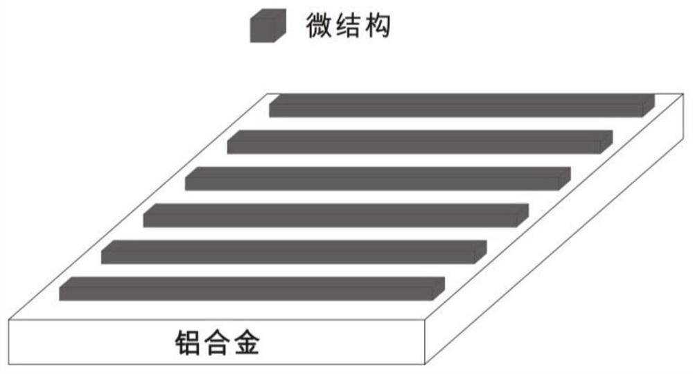
[0045] Step 2: If figure 1 As shown, it is planned to prepare array horizontal stripe microstructure, plan in the computer through the path planning software, set the laser scanning path as parallel strip scanning, the scanning distance is 150 μm, the layer thickness is 50 μm, and the number of printing layers is 1 layer ;

[0046] Step 3: Fix the 7075 aluminum alloy on the abutment in the forming cavity of the dual laser SLM equipment, and level the surface of the aluminum alloy at the Z-axis 0 point, so that the substrate serves as the forming plane;

[0047] Step 4: Fill 7075 aluminum alloy spherical powder around the aluminum alloy, and the particle size of the powder is between 15 μm and 60 μm;

[0048...

Embodiment 2

[0052] Step 1: Roughly polish the surface of 7075 aluminum alloy with a polishing machine to increase the adhesion between the powder and the surface, and clean it in ultrasonic for five minutes, then take it out, and dry the excess water on the surface with an air gun;

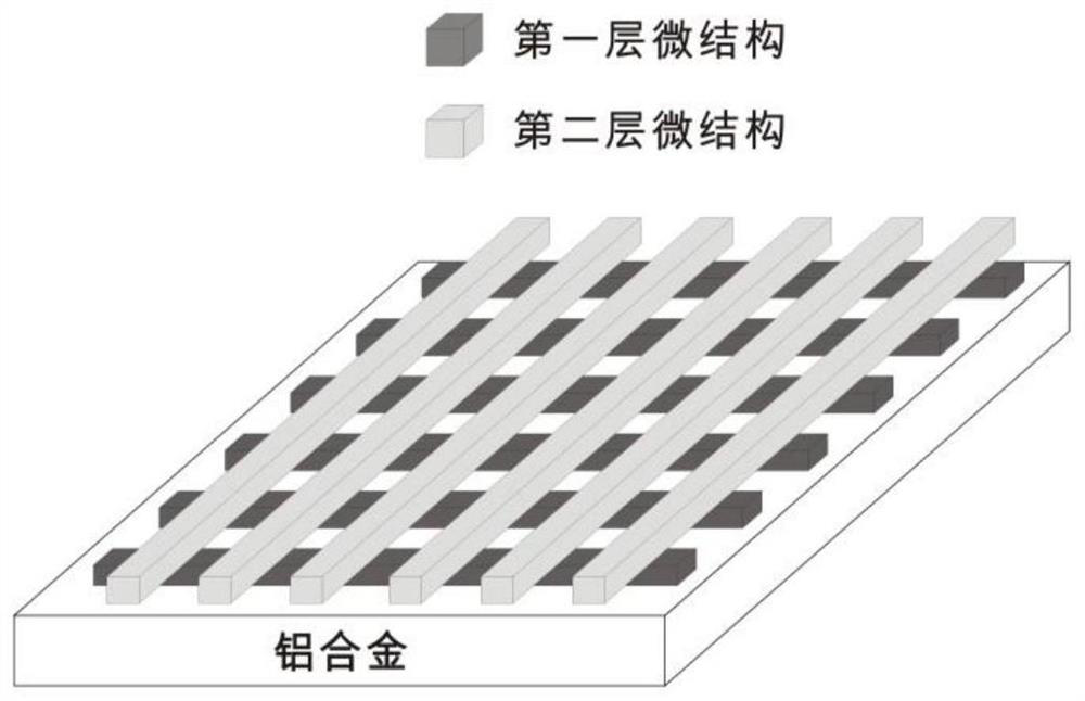
[0053] Step 2: If image 3 as shown, image 3 The middle part is to prepare the array hierarchical grid microstructure, which is planned in the computer through the path planning software. For the array hierarchical grid microstructure, the laser scanning path is set as parallel strip scanning, the scanning distance is 150 μm, and the layer thickness is 30 μm. , the number of printing layers is 2 layers, and the rotation angle between layers is 90°;

[0054] Step 3: Fix the 7075 aluminum alloy on the abutment in the forming cavity of the double laser SLM equipment, and use the surface of the aluminum alloy as the Z-axis 0 point for leveling;

[0055] Step 4: Fill 7075 aluminum alloy spherical powder around ...

Embodiment 3

[0060] Step 1: Roughly polish the surface of the stainless steel with a polishing machine to increase the adhesion between the powder and the surface, and clean it in ultrasonic for five minutes, then take it out, and dry the excess water on the surface with an air gun;

[0061] Step 2: To prepare the array hierarchical grid microstructure, plan in the computer through the path planning software, set the laser scanning path as parallel strip scanning, the scanning distance is 100 μm, the layer thickness is 80 μm, and the number of printing layers is 2 layers , the rotation angle between layers is 120°;

[0062] Step 3: Fix the stainless steel on the abutment in the forming cavity of the double laser SLM equipment, and use the stainless steel surface as the Z-axis 0 point for leveling;

[0063] Step 4: Fill Ti6Al4V powder around the stainless steel, the powder particle size is 15μm~60μm;

[0064] Step 5: Pour the above-mentioned Ti6Al4V powder into the powder cylinder of the l...


PUM

PropertyMeasurementUnit
particle diameteraaaaaaaaaa
widthaaaaaaaaaa

Abstract

The present invention is a technical field prepared on the surface microstructure, and a method and product of a multi -level microstructure of metal surfaces are disclosed.When the micro -structured substrate is set on the substrate, it is a single layer or a multi -layer structure. The width of the rules and orderly distribution in each layer of micro -structures is less than a bar -shaped microcontroller of 200 μm.) Divide the substrate on the surface; divide the slicing layer according to the number of layers of the micro -structure to be formed, set the layer of the layer of the powder, plan the forming path of the slicing layer, (b) use the substrate as a forming plane, from the bottom up layer by layer by layer by layer by layer.The laser constituency melted the forming layer to obtain the required micro -structures on the substrate.Through the present invention, the large -scale metal surface rules are used in an orderly and multi -level micro -structures to be prepared in an orderly manner. It is suitable for a variety of common metal materials such as titanium alloy, aluminum alloy, stainless steel, and nickel -based alloy, and the process is simple.

Description

technical field [0001] The invention belongs to the technical field of surface microstructure preparation, and more specifically relates to a forming method and product of a multilevel microstructure on a metal surface. Background technique [0002] Surface microstructure preparation technology can play an important role in changing the surface characteristics of materials. By preparing microstructures on the surface of materials, special functions can be endowed on materials, surface function modification can be realized, and the original performance of materials can be improved. Therefore, it has great potential in various fields. Value. The preparation of surface microstructures has gone through decades since it was proposed, and it has been involved in many fields such as medicine, biology, sensors, architecture, aerospace, etc., and solves various problems for human beings in life and industry. [0003] At present, the preparation methods of metal surface microstructur...

Claims


Application Information

Patent Timeline
Patent Type & Authority Patents(China)
IPC IPC(8): B22F3/105
CPCB22F10/00B22F10/38B22F10/366B22F10/28B22F10/36B22F12/41Y02P10/25
Inventor 张李超汤名锴史玉升
Owner HUAZHONG UNIV OF SCI & TECH
Why Eureka
Try Eureka