Wave absorbing structure

A wave structure and support layer technology, applied in the field of wave-absorbing materials, can solve the problems of wave incident angle sensitivity and narrow action frequency band, and achieve the effect of wide absorption frequency band, high absorption efficiency, and better design

Inactive Publication Date: 2019-09-27
AIR FORCE UNIV PLA
View PDF4 Cites 2 Cited by
  • Summary
  • Abstract
  • Description
  • Claims
  • Application Information

AI Technical Summary

Problems solved by technology

At present, research on wave-absorbing materials based on metamaterials has also attracted much attention. Metamaterials refer to a type of artificial composite structure or composite material with extraordinary electromagnetic properties that natural materials do not have. In 2008, researchers proposed a metamaterial electromagnetic wave absorber. Based on the concept of designing the key physical dimensions of metamaterials to

Method used


Image

  • Wave absorbing structure
  • Wave absorbing structure
  • Wave absorbing structure

Examples


Example Embodiment

[0024] Example 1

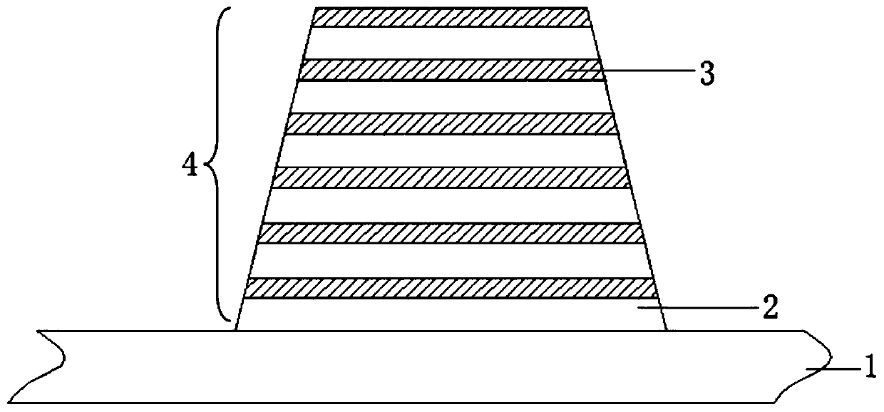
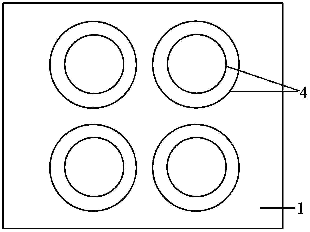
[0025] like figure 1 and figure 2 As shown, the absorbing structure of this embodiment includes a support layer 1 and a plurality of superatoms 4 arranged in an array on the support layer 1, and the superatoms 4 are periodically formed by the dielectric layer 2 and the metal layer 3 from bottom to top. Superimposed to form a conical structure, the material of the support layer 1 is epoxy glass FR-4, the dielectric constant is 4, and the thickness is 2mm; the material of the dielectric layer 2 is epoxy glass FR-4, and the thickness is 0.182mm The metal layer 3 is made of copper with a thickness of 0.036mm; the number of layers of the dielectric layer 2 and the metal layer 3 periodically stacked is 29 layers; the bottom diameter of the superatom 4 is 25mm, and the top diameter is 12mm ; The distance between the centerlines of the adjacent superatoms 4 is 24mm.

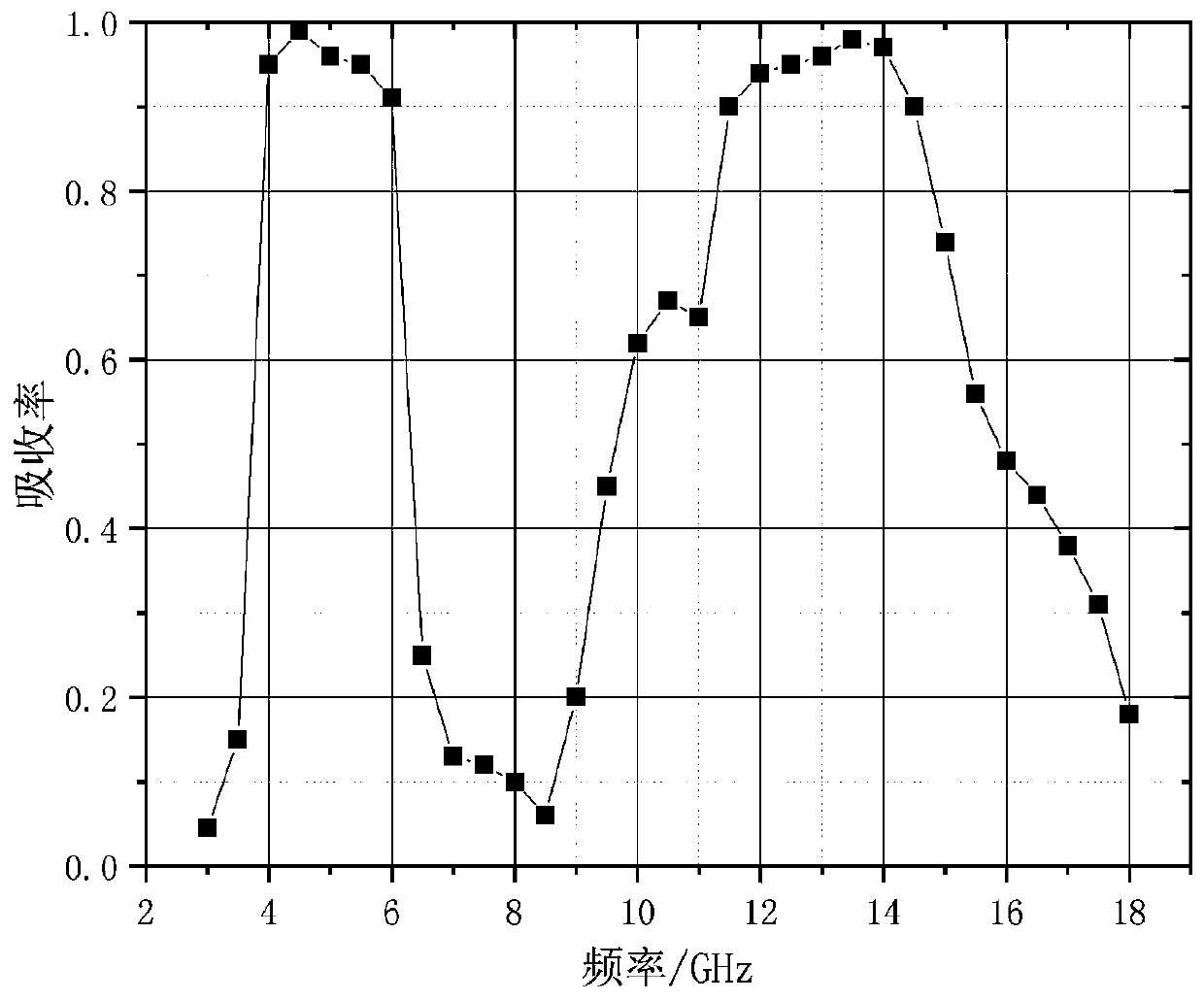
[0026] When microwave electromagnetic radiation is incident on the surface of the wave-absorbin...

Example Embodiment

[0028] Example 2

[0029] like figure 1 and figure 2 As shown, the absorbing structure of this embodiment includes a support layer 1 and a plurality of superatoms 4 arranged in an array on the support layer 1, and the superatoms 4 are periodically formed by the dielectric layer 2 and the metal layer 3 from bottom to top. Superimposed to form a conical structure, the material of the support layer 1 is silicon, and the thickness is 100nm; the material of the dielectric layer 2 is silicon, and the thickness is 40nm; the material of the metal layer 3 is gold, and the thickness is 5nm; The number of layers of dielectric layer 2 and metal layer 3 stacked periodically is 4 layers; the diameter of the bottom of the superatom 4 is 350mm, and the diameter of the top is 220mm; the distance between the centerlines of the adjacent superatoms 4 is 400nm.

[0030] When infrared and visible light electromagnetic radiation is incident on the surface of the wave-absorbing structure of this e...

Example Embodiment

[0031] Example 3

[0032] like figure 1 and figure 2As shown, the absorbing structure of this embodiment includes a support layer 1 and a plurality of superatoms 4 arranged in an array on the support layer 1, and the superatoms 4 are periodically formed by the dielectric layer 2 and the metal layer 3 from bottom to top. Superimposed to form a conical structure, the material of the support layer 1 is epoxy glass FR-4, the dielectric constant is 4, and the thickness is 2mm; the material of the dielectric layer 2 is epoxy glass FR-4, and the thickness is 0.1mm The material of the metal layer 3 is silver, with a thickness of 0.01mm; the number of layers of the dielectric layer 2 and the metal layer 3 periodically stacked is 50 layers; the bottom diameter of the superatom 4 is 25mm, and the top diameter is 12mm ; The distance between the centerlines of the adjacent superatoms 4 is 50mm.

[0033] When microwave electromagnetic radiation is incident on the surface of the wave-abs...


PUM

PropertyMeasurementUnit
Thicknessaaaaaaaaaa
Thicknessaaaaaaaaaa
Thicknessaaaaaaaaaa

Abstract

The invention provides a wave absorbing structure, and the structure comprises a supporting layer and a plurality of superatoms which are arranged on the supporting layer and distributed in an array mode, wherein the superatoms are of a circular-truncated-cone-shaped structure formed by periodically overlapping a dielectric layer and a metal layer from bottom to top. According to the wave absorbing structure, the sensitivity of the wave absorbing characteristic to the electromagnetic radiation polarization angle can be inhibited; a fundamental frequency magnetic resonance and third-order magnetic resonance action mechanism forms localized and non-localized plasma waves in a plurality of superatoms arranged in an array; therefore, the absorption structure has two absorption bands at the same time, the absorption frequency band of the wave absorption structure is wide, the absorption efficiency is high, and the design of the light absorption characteristic of the wave absorption structure is more flexible and tunable.

Description

technical field [0001] The invention belongs to the technical field of wave-absorbing materials, and in particular relates to a wave-absorbing structure. Background technique [0002] With the development of modern science and technology, the influence of electromagnetic wave radiation on the environment is increasing day by day. Airplane flights at airports are often delayed due to electromagnetic wave interference, and interference sources such as mobile phones in hospitals often interfere with the normal work of various electronic medical instruments. Therefore, searching for absorbing materials that can efficiently weaken electromagnetic radiation has become a major topic in the field of electromagnetic protection technology such as electromagnetic pollution control. According to the material forming process, the absorbing material can be divided into coating type and structural type; and according to the loss mechanism, the absorbing material can be divided into resist...

Claims


Application Information

Patent Timeline
IPC IPC(8): H05K9/00G02B5/00
CPCG02B5/008H05K9/0081
Inventor 康轶凡周九茹张利霞
Owner AIR FORCE UNIV PLA
Why Eureka
Try Eureka