Packaging method of MEMS sensor
A packaging method and sensor technology, applied in the field of MEMS, can solve the problems of excessive packaging shell cost and lower sensor performance, and achieve the effects of expanding the use range of devices, enhancing mechanical protection, and improving performance
- Summary
- Abstract
- Description
- Claims
- Application Information
AI Technical Summary
Problems solved by technology
Method used
Image

Examples
Embodiment 1
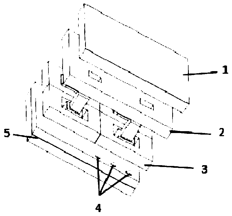
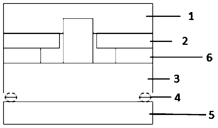
[0042] A method for encapsulating a MEMS sensor, the prepared MEMS sensor such as figure 1 with figure 2 As shown, the method includes the following steps:
[0043] 1. Handling of multilayer circuit boards 5
[0044] A multi-layer circuit board 5 is selected, cleaned and dried, and lead pads are printed on the multi-layer circuit board by screen printing technology, and gold balls 4 are welded on the pads for lead wires.
[0045] Wherein, the multilayer circuit board of the present embodiment has not been subjected to solder resist treatment; the specific process steps of the screen printing technology are: printing the solder resist ink onto the layout of the multilayer circuit board 5 through a screen, and printing the solder resist ink on the layout of the multilayer circuit board 5 at a certain temperature, time and ventilation Under the condition of a certain amount, the solvent in the ink is initially volatilized, and then the required pads and through holes are prote...
Embodiment 2
[0067] This embodiment is a packaging method for MEMS sensors, the main steps are the same as in Embodiment 1, the difference lies in the process parameters in the preparation process; specifically:
[0068] A method for encapsulating a MEMS sensor, the prepared MEMS sensor such as figure 1 with figure 2 As shown, the method includes the following steps:
[0069] 1. Handling of multilayer circuit boards 5
[0070] A multi-layer circuit board 5 is selected, cleaned and dried, and lead pads are printed on the multi-layer circuit board by screen printing technology, and gold balls 4 are welded on the pads for lead wires.
[0071] Wherein, the multilayer circuit board of the present embodiment has not been subjected to solder resist treatment; the specific process steps of the screen printing technology are: printing the solder resist ink onto the layout of the multilayer circuit board 5 through a screen, and printing the solder resist ink on the layout of the multilayer circui...
Embodiment 3
[0085] This embodiment is a packaging method for MEMS sensors, the main steps are the same as in Embodiment 1, the difference lies in the process parameters in the preparation process; specifically:
[0086] A method for encapsulating a MEMS sensor, the prepared MEMS sensor such as figure 1 with figure 2 As shown, the method includes the following steps:
[0087] 1. Handling of multilayer circuit boards 5
[0088] A multi-layer circuit board 5 is selected, cleaned and dried, and lead pads are printed on the multi-layer circuit board by screen printing technology, and gold balls 4 are welded on the pads for lead wires.
[0089] Wherein, the multilayer circuit board of the present embodiment has not been subjected to solder resist treatment; the specific process steps of the screen printing technology are: printing the solder resist ink onto the layout of the multilayer circuit board 5 through a screen, and printing the solder resist ink on the layout of the multilayer circui...
PUM
| Property | Measurement | Unit |
|---|---|---|
| Thickness | aaaaa | aaaaa |
| Thickness | aaaaa | aaaaa |
| Thickness | aaaaa | aaaaa |
Abstract
Description
Claims
Application Information
 - R&D
- Intellectual Property
- Life Sciences
- Materials
- Tech Scout
- Unparalleled Data Quality
- Higher Quality Content
- 60% Fewer Hallucinations
Browse by: Latest US Patents, China's latest patents, Technical Efficacy Thesaurus, Application Domain, Technology Topic, Popular Technical Reports.
© 2025 PatSnap. All rights reserved.Legal|Privacy policy|Modern Slavery Act Transparency Statement|Sitemap|About US| Contact US: help@patsnap.com